

Introduction
In this teardown, we are examining the AOOSTAR AG01 OCuLink eGPU Dock. Hooking up to laptops or mini PCs via a high-speed OCuLink interface, this dock unlocks PCIe 4.0×4 bandwidth. Housed in a sleek aluminum alloy shell with a built-in power unit, it combines clean aesthetics with a compact footprint. Inside, it packs a reliable 400W Huntkey power supply that broadly supports NVIDIA, AMD, and Intel desktop GPUs.
On the hardware side, the AOOSTAR AG01 features dual 8-pin power headers on the dock body, supplying juice to the graphics card via the bundled power harness. The GPU plugs straight into the onboard PCIe slot and is anchored securely using the dock's integrated mounting screws. Next, let's join ChargerLAB as we strip down this AOOSTAR graphics dock to check out its internal engineering and component choices.
Product Appearance

The AOOSTAR AG01 GPU dock comes in a cardboard box.
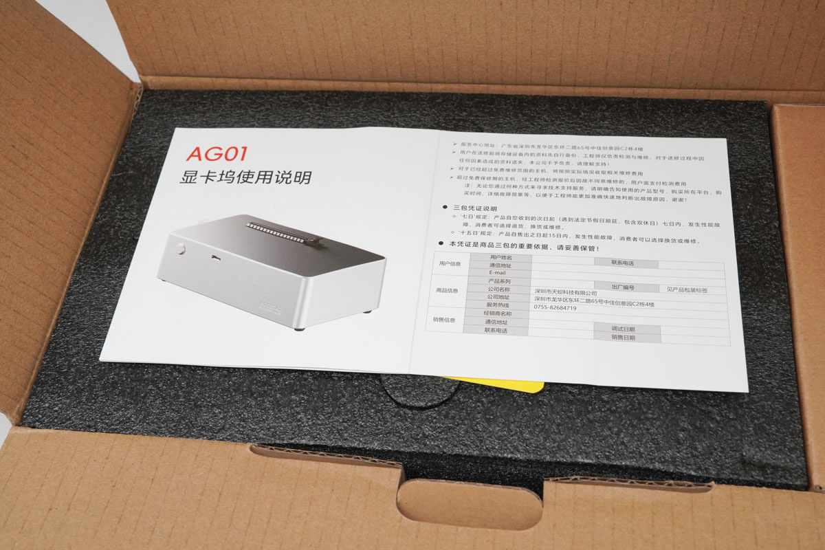
An instruction manual is included.
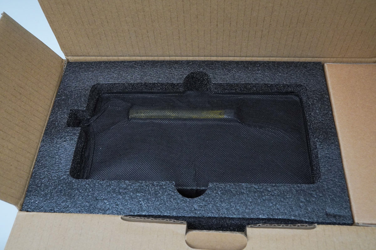
Foam inserts provide cushioning during transport.
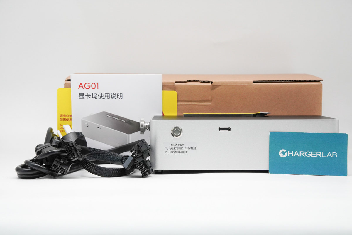
The AC power cable, GPU power cable, and external GPU dock.
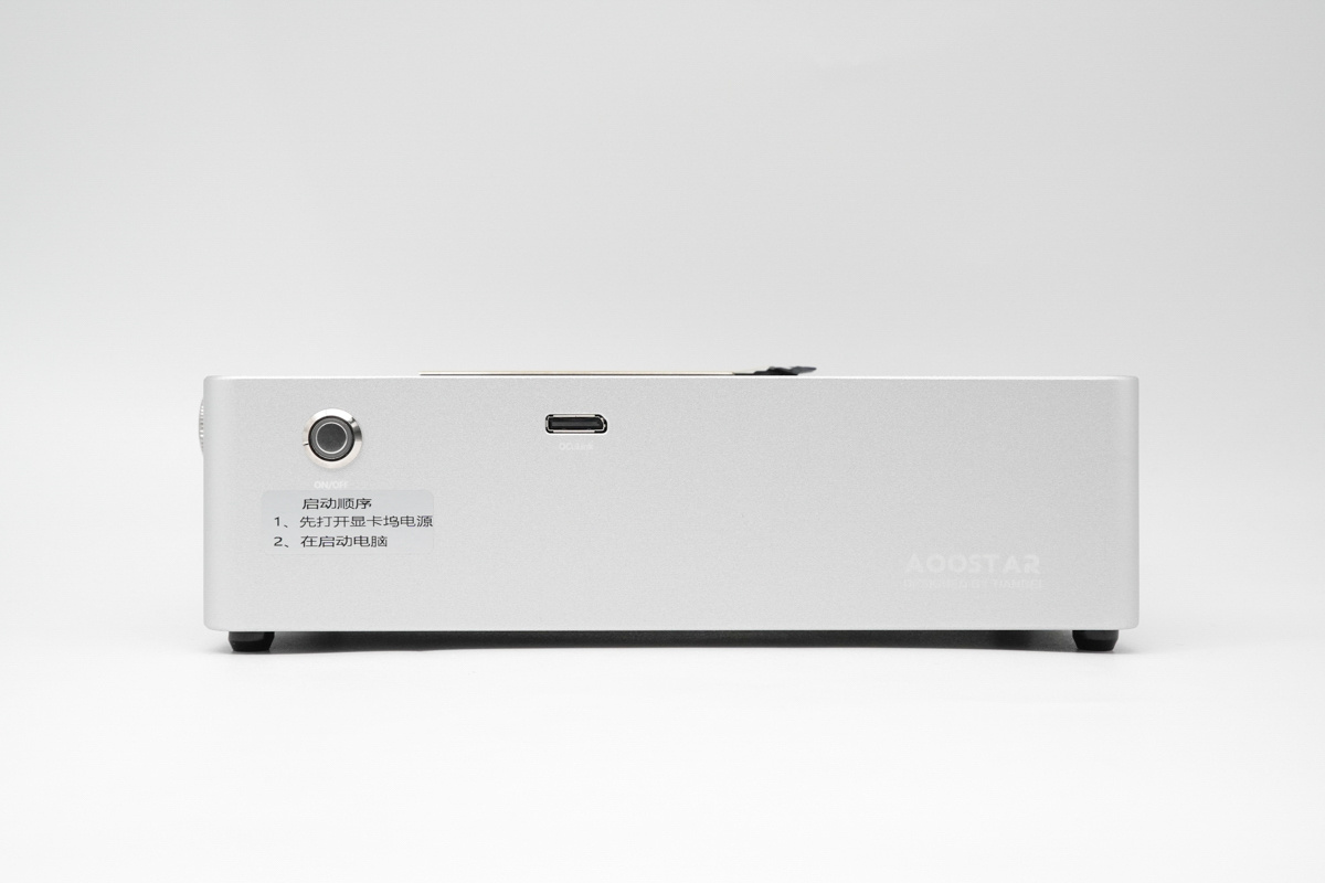
One side of the dock features a power switch and an OCuLink port.
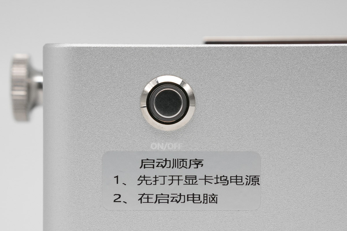
A startup sequence label is attached below the power switch, instructing users to turn on the GPU dock before starting the computer.
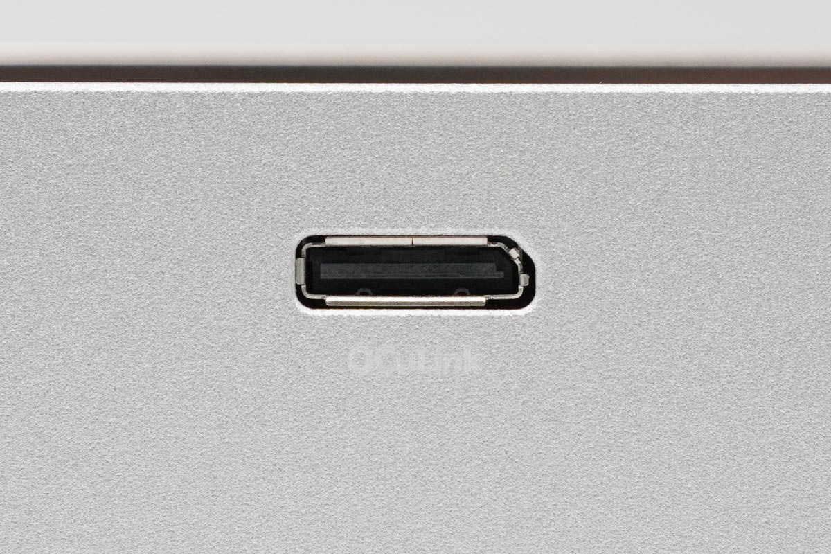
The OCuLink port.

The AOOSTAR logo is printed on the enclosure.
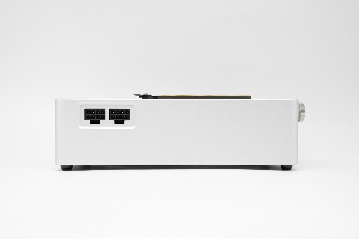
The opposite side of the dock features GPU power connectors.
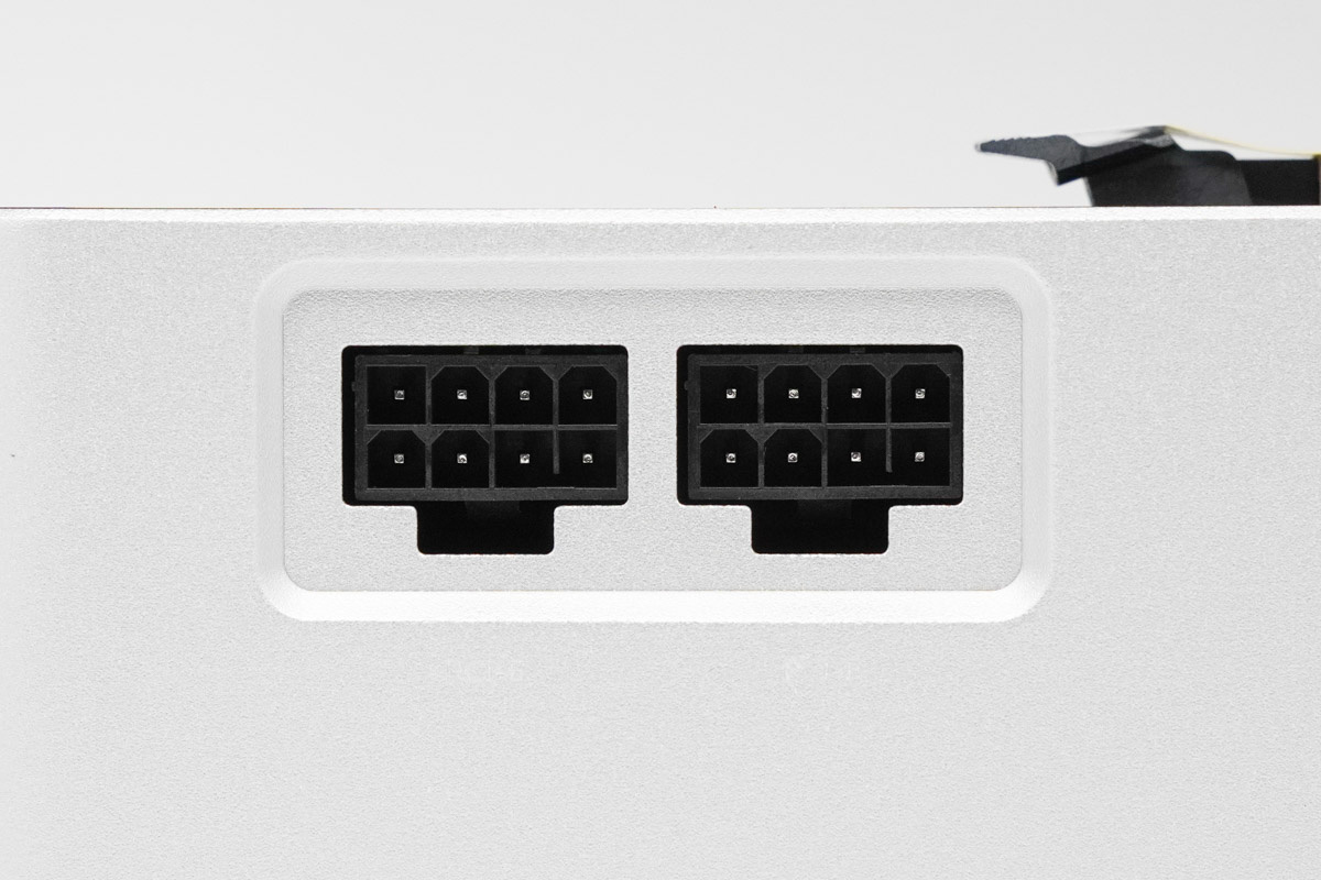
The dual 8-pin GPU power connectors.
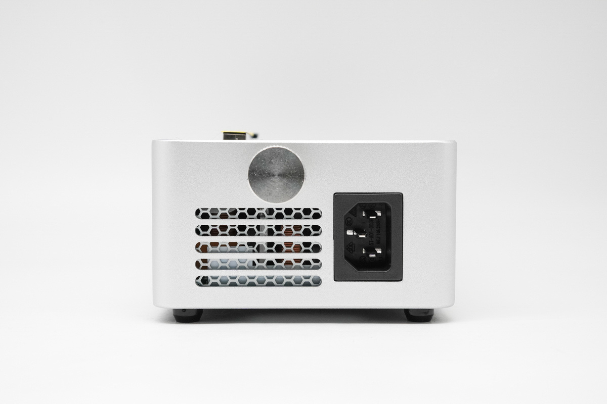
The side of the dock features a retaining screw, ventilation openings, and an AC power inlet.
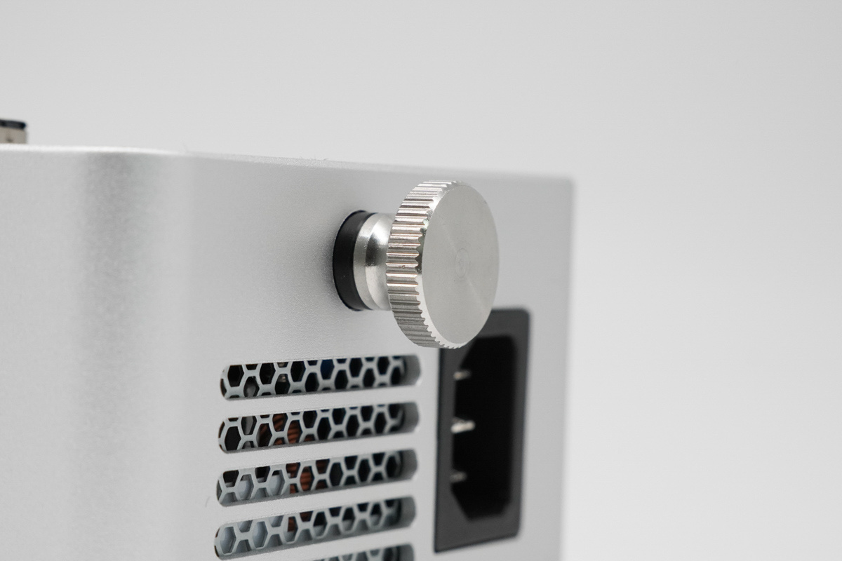
The hand-tightened retaining screw secures the graphics card.
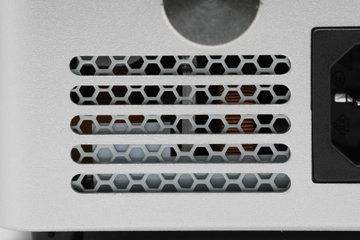
A protective grille is installed behind the ventilation openings to prevent foreign objects from entering.
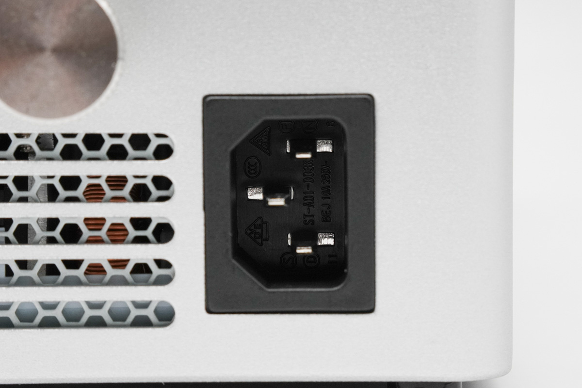
The three-pin AC power inlet.
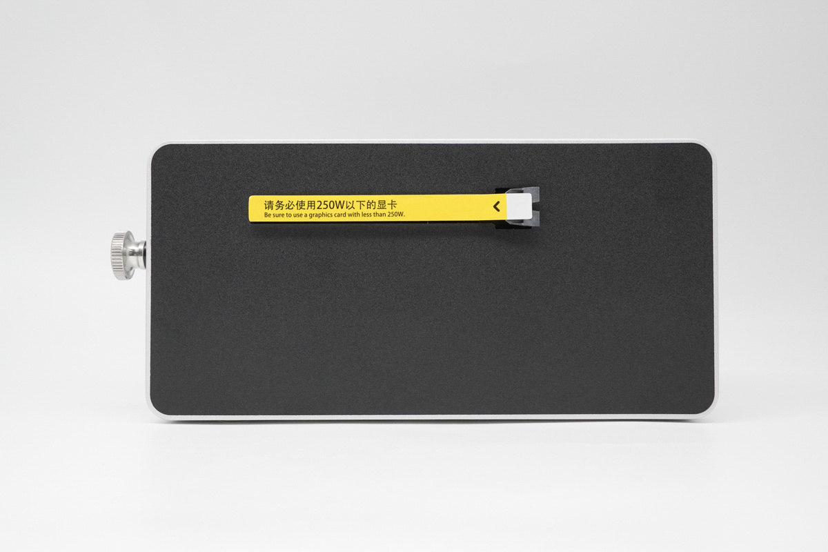
A label is attached to the PCIe slot, instructing users to use graphics cards rated below 250W.
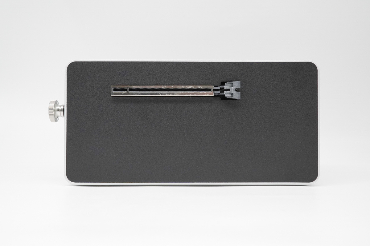
The PCIe slot is located beneath the label.
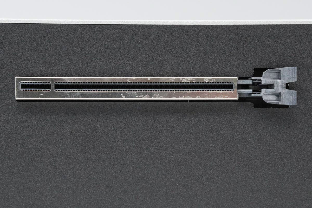
The PCIe slot features a metal housing.
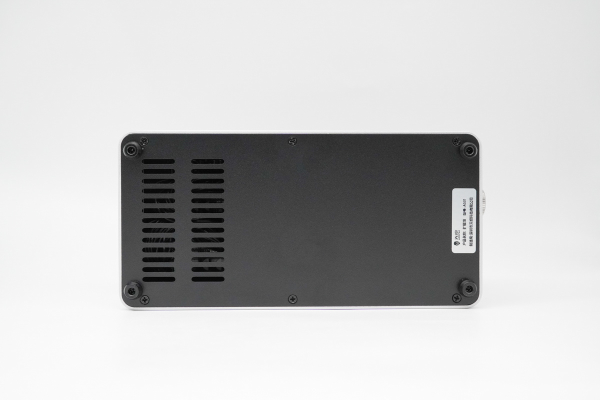
The bottom of the dock features ventilation openings and rubber feet.
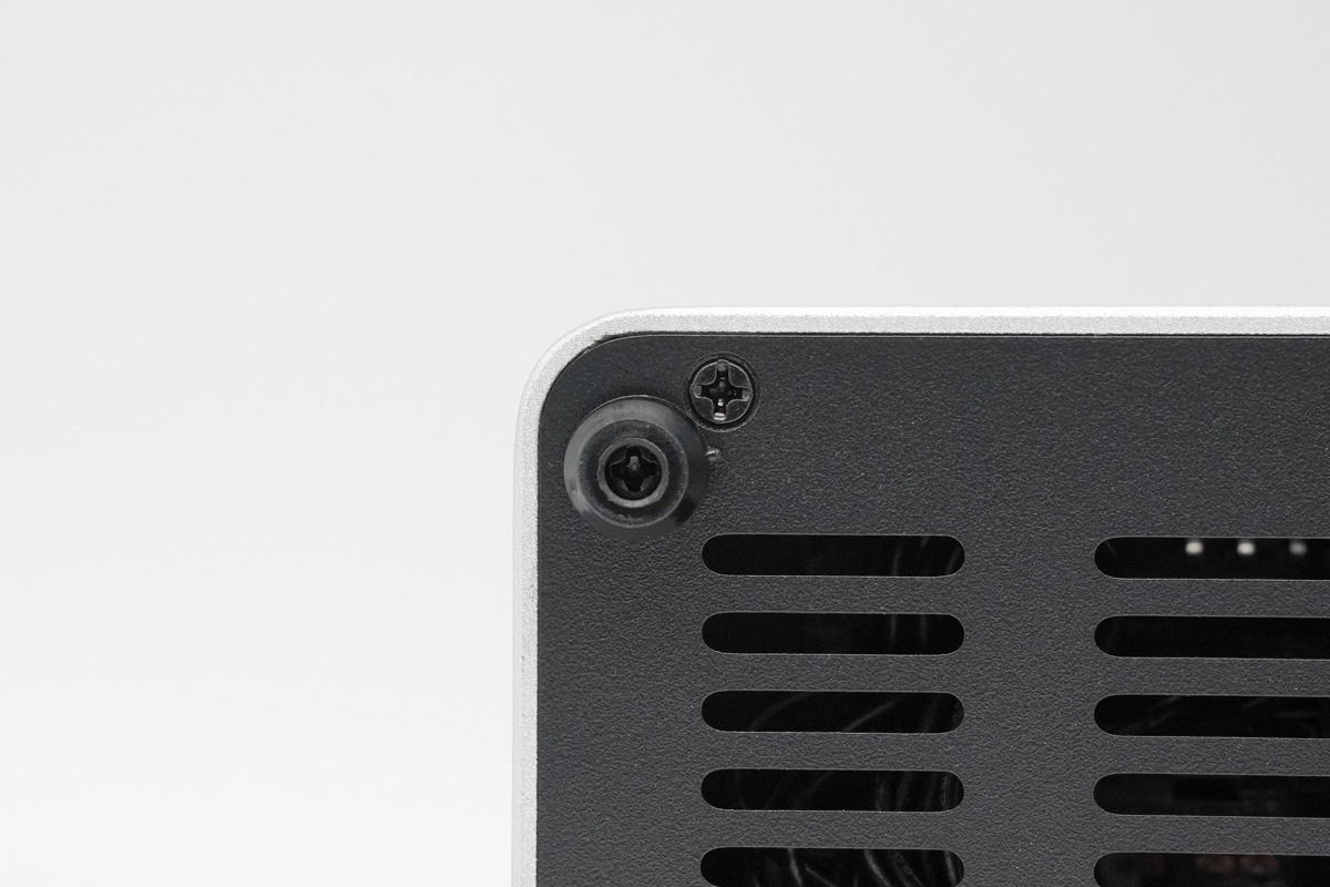
The rubber feet and bottom cover are secured with screws.
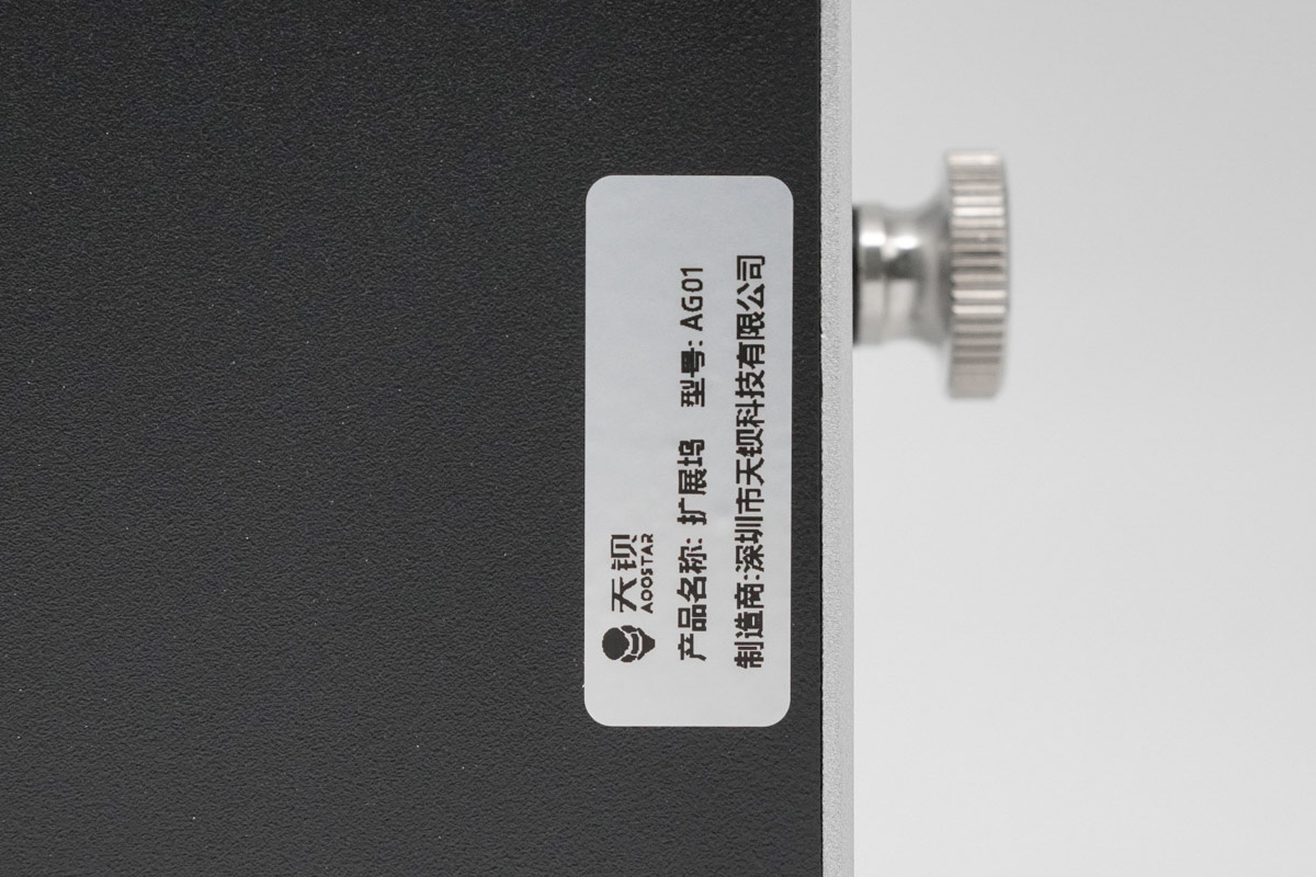
A label on the bottom cover provides the brand, product name, and manufacturer info.

The length of the dock is about 220mm (8.661 inches).
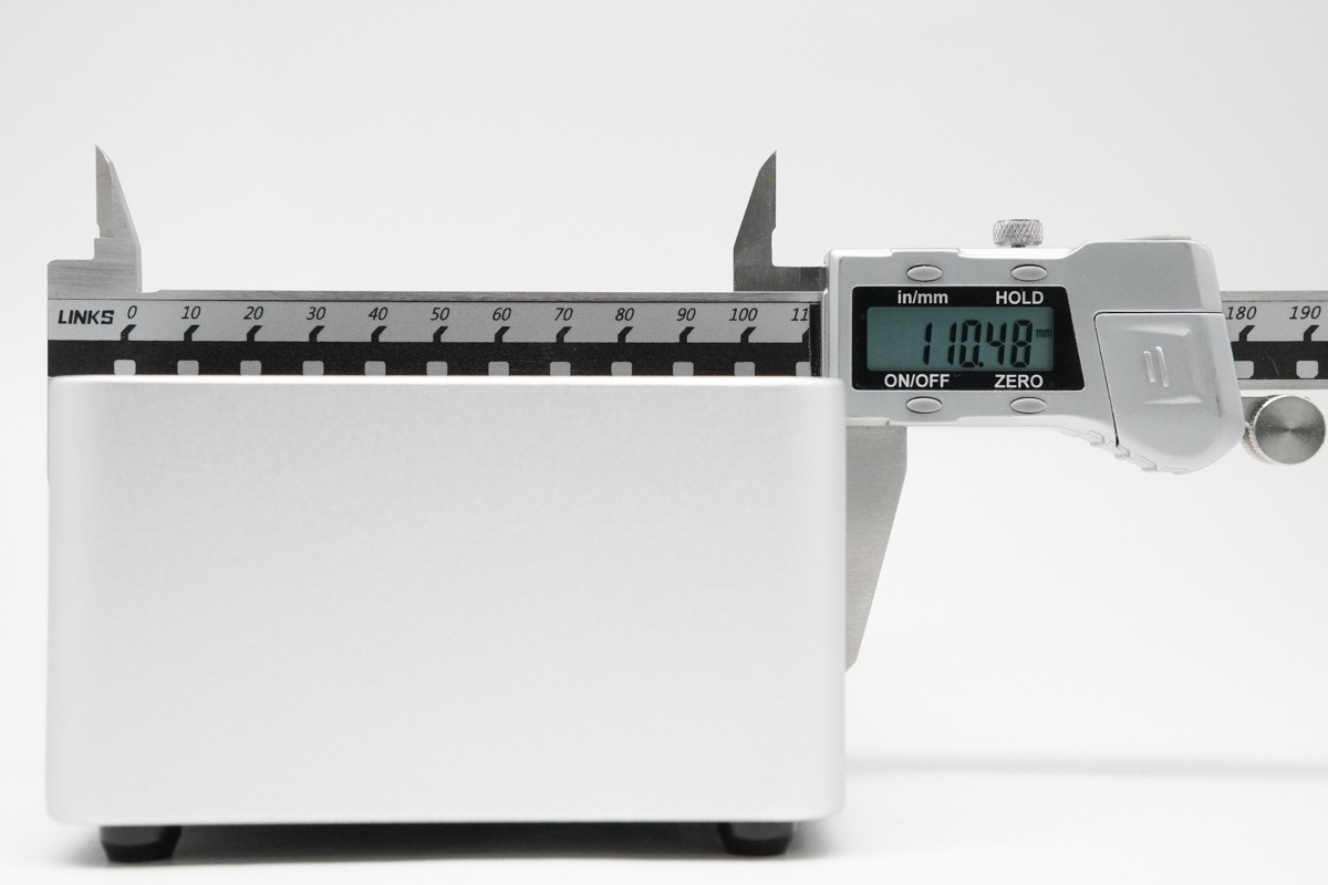
The width of the dock is about 110.5mm (4.350 inches).
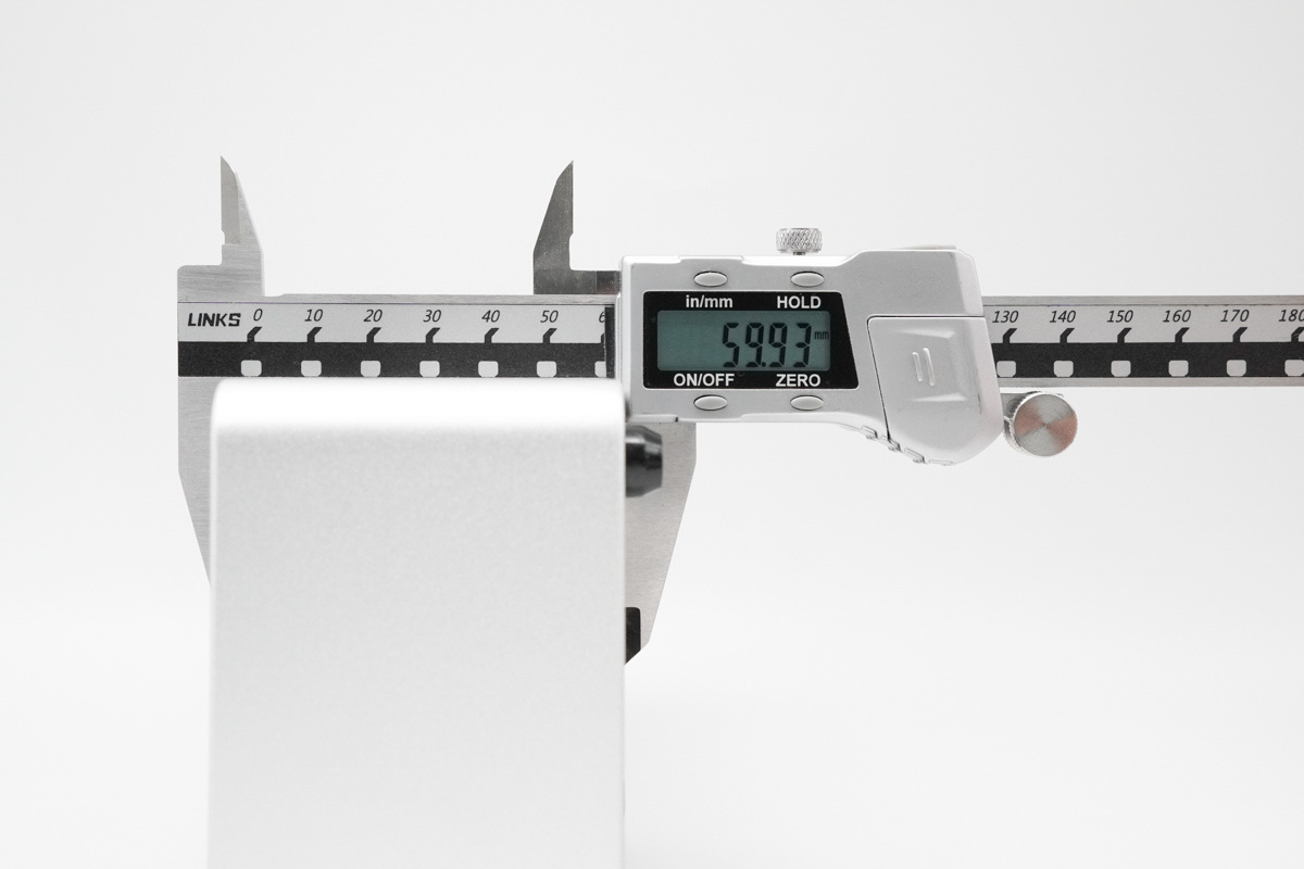
The thickness of the dock is about 60mm (2.362 inches).
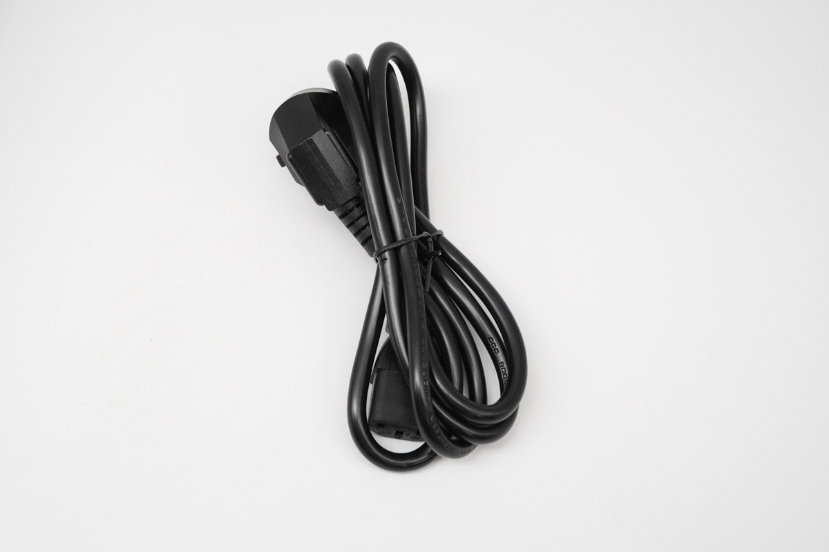
An AC power cable is included with the GPU dock.
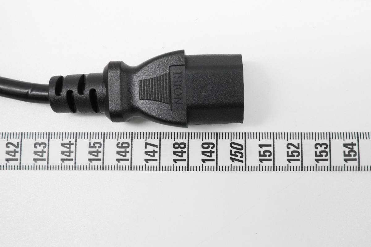
The length of the AC power cable is about 150cm (59.055 inches).
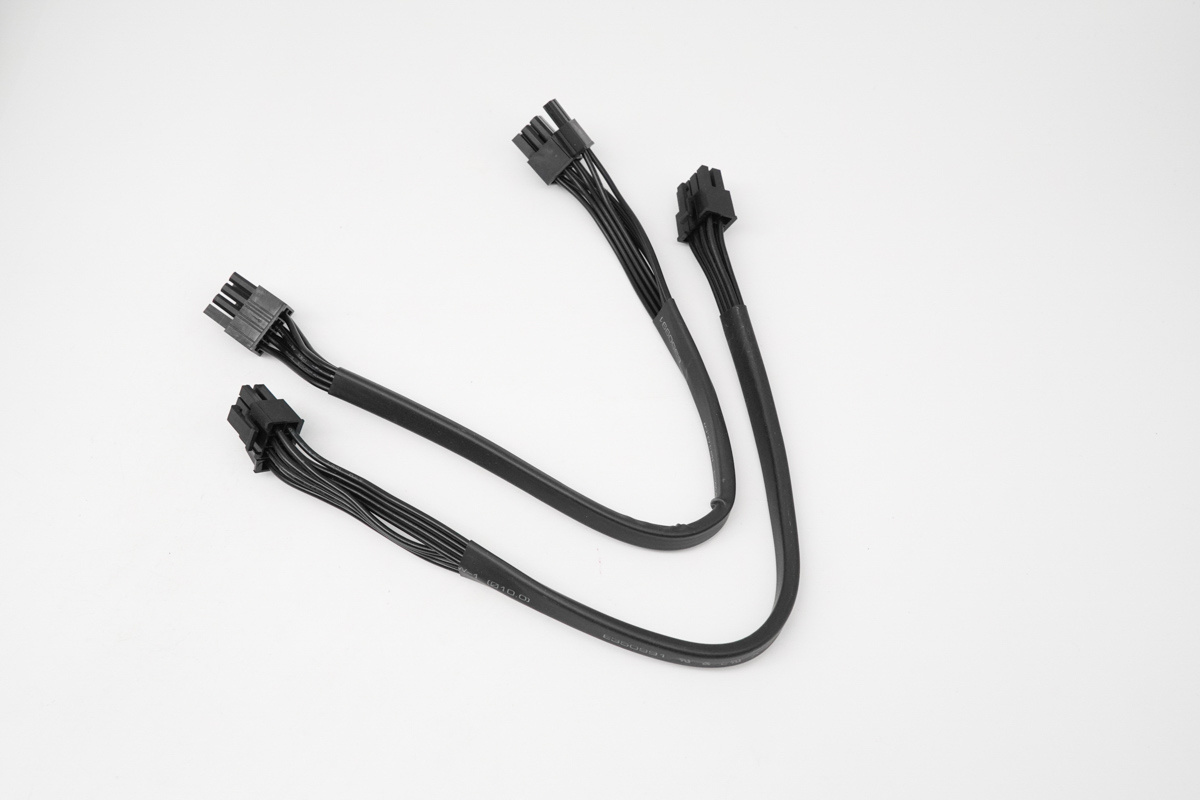
Two dual 8-pin GPU power cables.
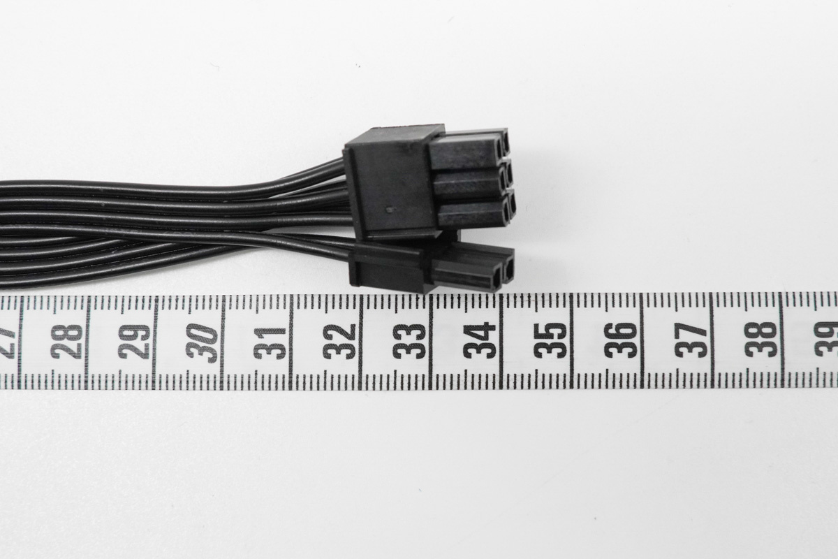
The length of the GPU power cable is about 34cm (13.386 inches).
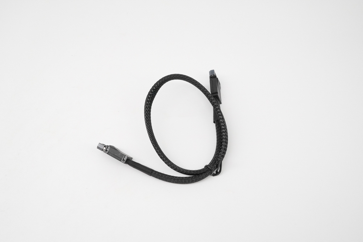
The OCuLink cable.
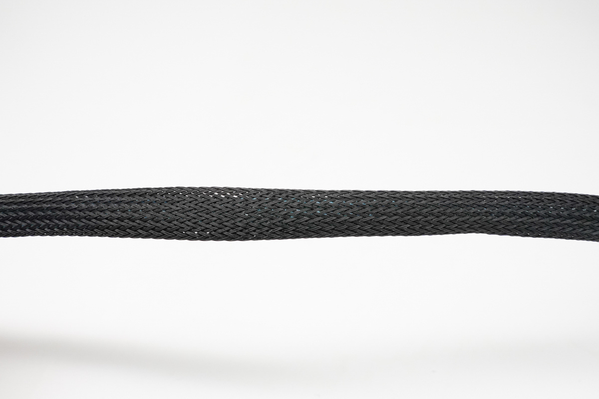
The OCuLink cable features protective sleeving.
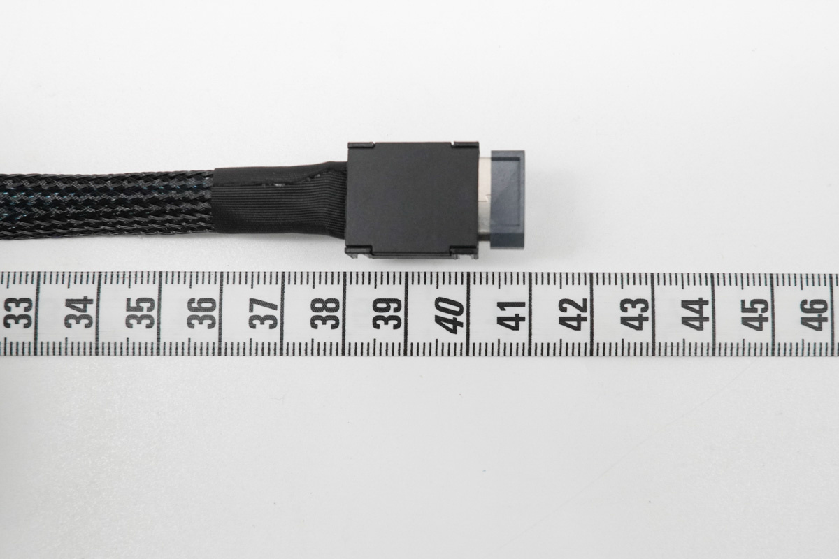
The length of the OCuLink cable is about 41cm (16.142 inches).
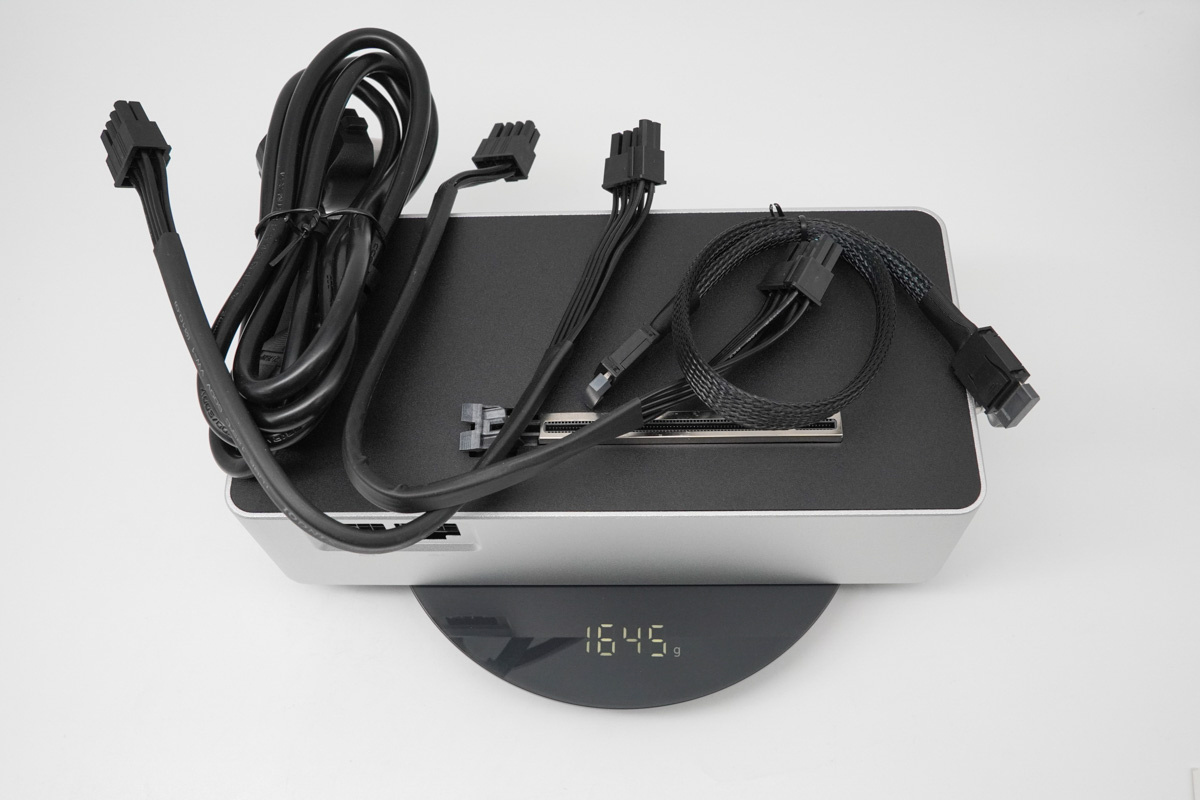
The weight is about 14645g (516.588 oz).
Teardown
After looking at the graphics card dock's unboxing and exterior, let's take it apart and examine its internal design and components.
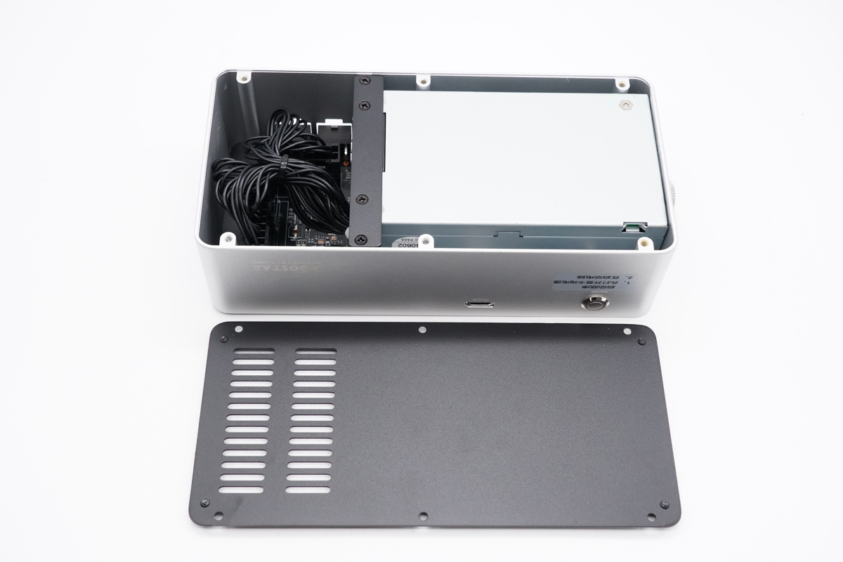
First, remove the screws securing the rear cover and take off the cover.
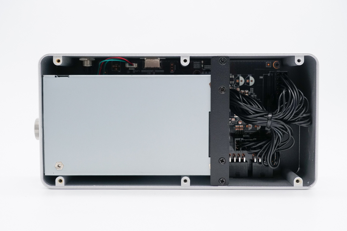
A power supply module is installed inside the rear cover and secured with a metal retaining plate and screws.
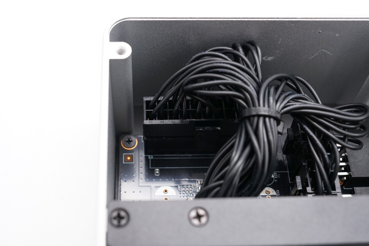
The power supply module connects to the mainboard of the dock through a connector.
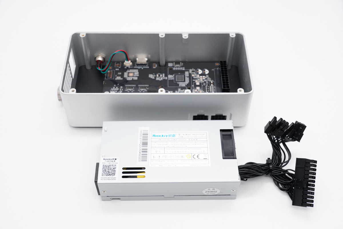
Remove the power supply module from the enclosure.
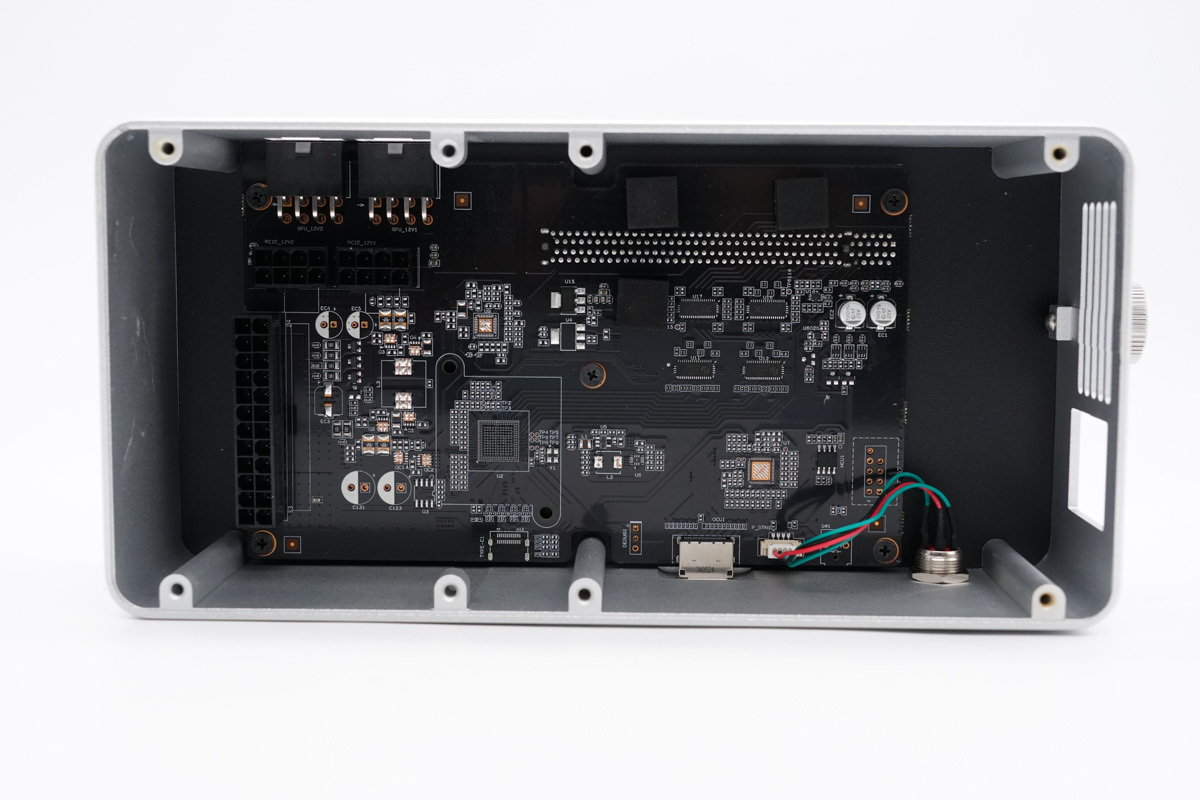
The enclosure houses the dock's PCBA module, which is secured with screws.
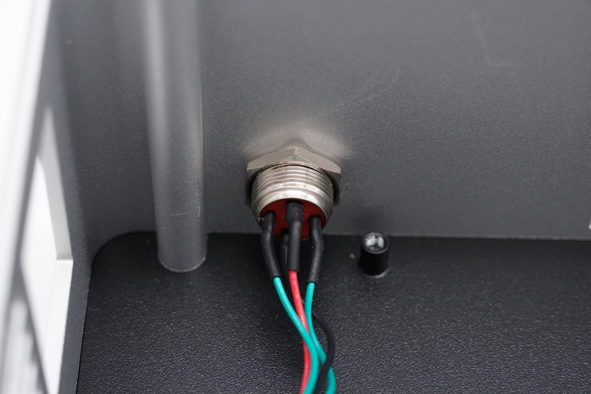
The power button has a built-in indicator LED and is connected via soldered wires. The pins are insulated with heat-shrink tubing.
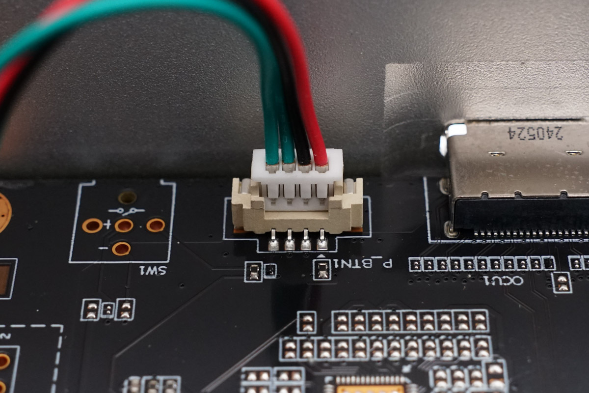
The other end connects to the PCBA module through a connector.
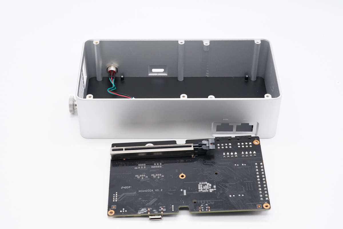
Remove the securing screws and take out the PCBA module.
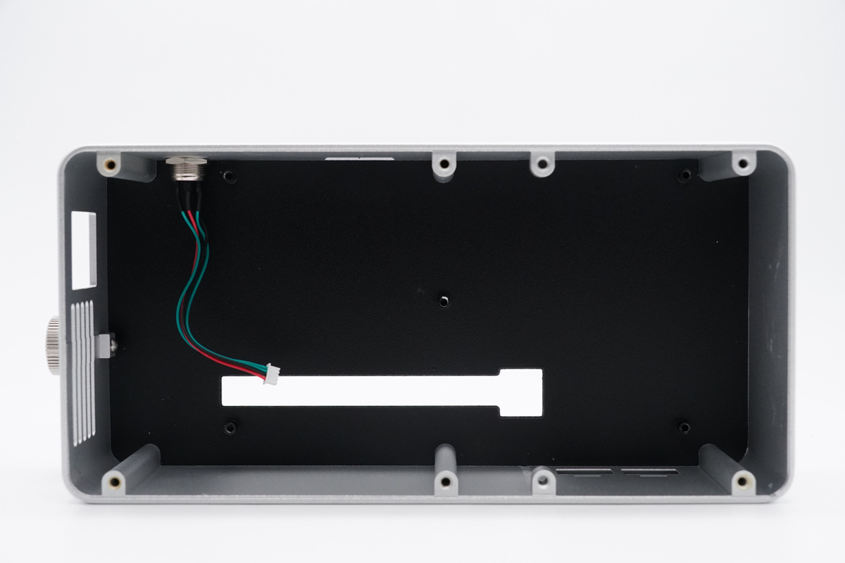
Screw posts are provided inside the panel to secure the PCBA module.
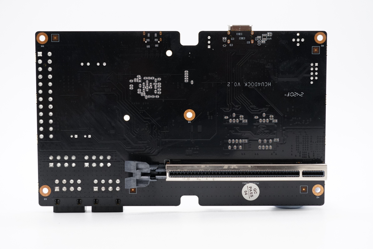
A PCIe slot is soldered onto the front of the PCBA module.
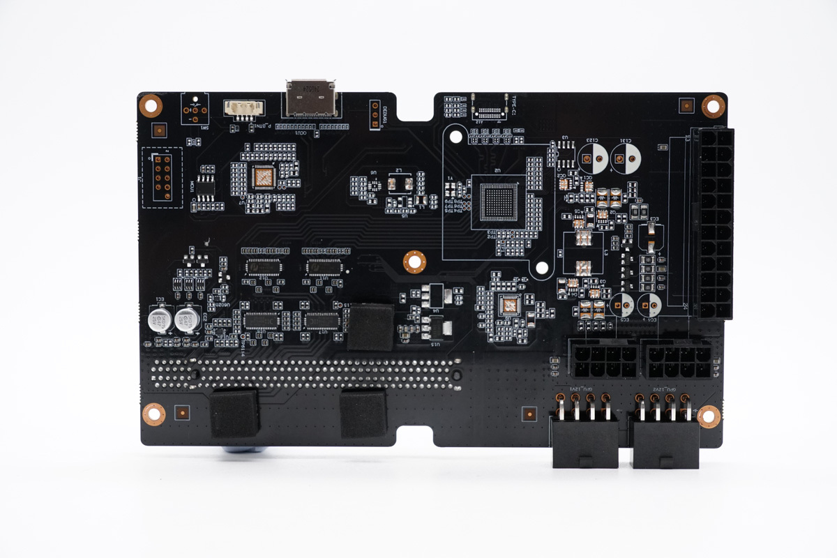
A multiplexer and ReDriver chip are installed on the left of the PCBA, while footprints for a USB-C receptacle and Thunderbolt controller are reserved on the right.
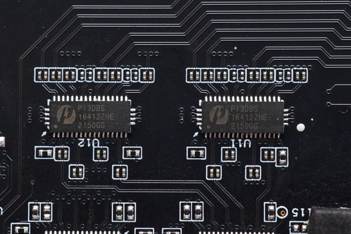
The multiplexer is from DIODES, model PI3DBS16412. It is a 2:1 multiplexer switch with four differential channels, designed for applications including PCIe 4.0, USB 3.0, USB 3.1, 10GbE, Thunderbolt 3, and SAS 3.0. It supports data rates of up to 20Gbps and bidirectional operation, and is housed in a TQFN42 package. It is used for switching between the OCuLink and Thunderbolt connections.
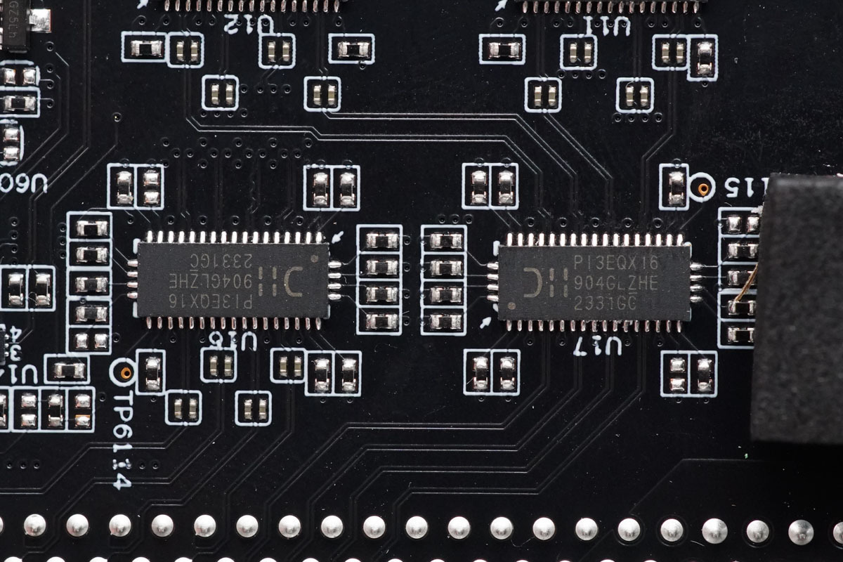
The ReDriver chip is from DIODES, model PI3EQX16904GL. It provides programmable linear equalization to optimize signal integrity, supports four differential channels and serial links operating at 2.5–16Gbps, and is housed in a TQFN-42 package.
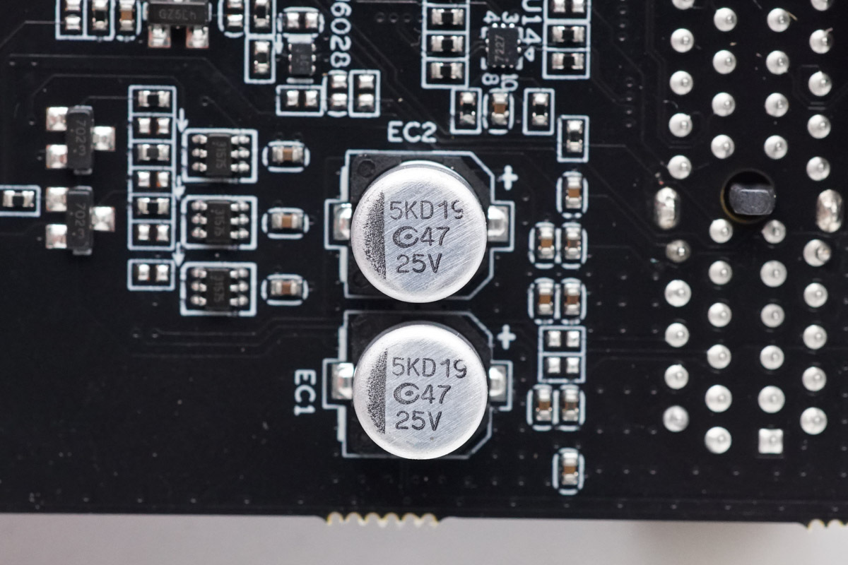
The filter cap is from APAQ, spec 47μF 25V.
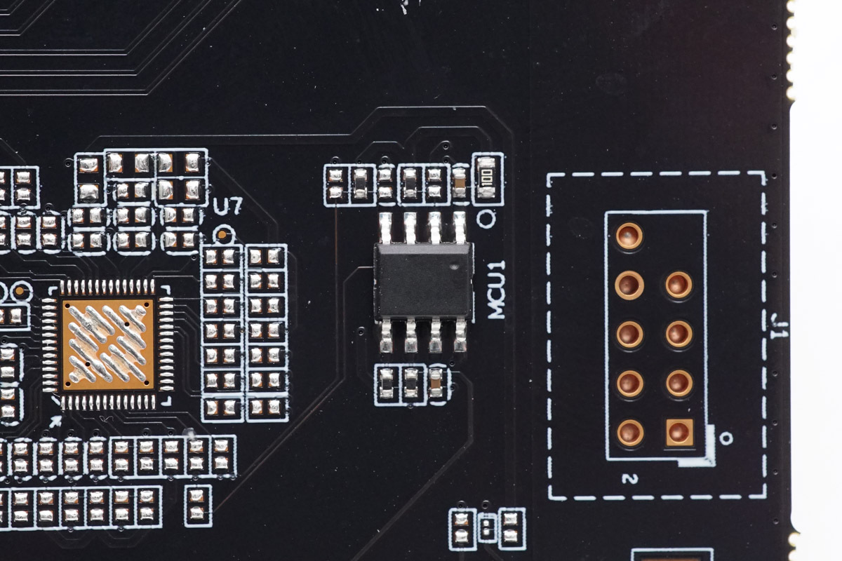
The unmarked MCU in an SOP8 package.
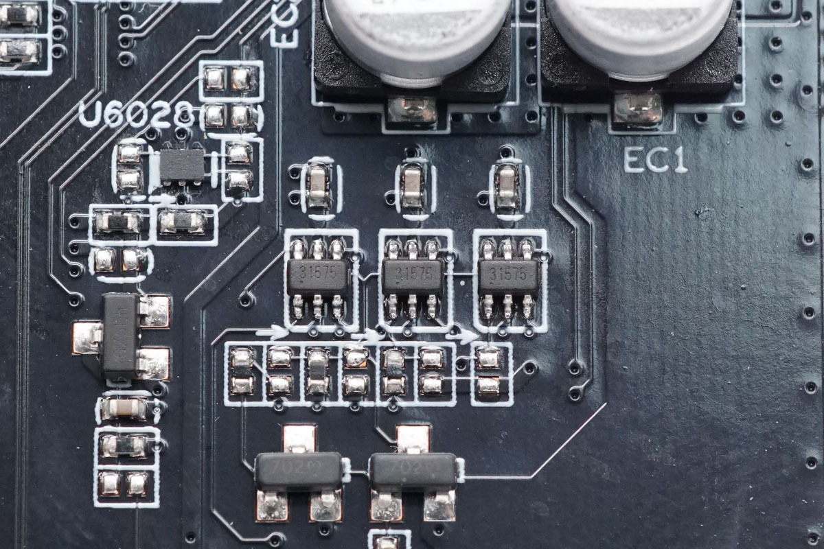
The switching ICs, marked 31575.
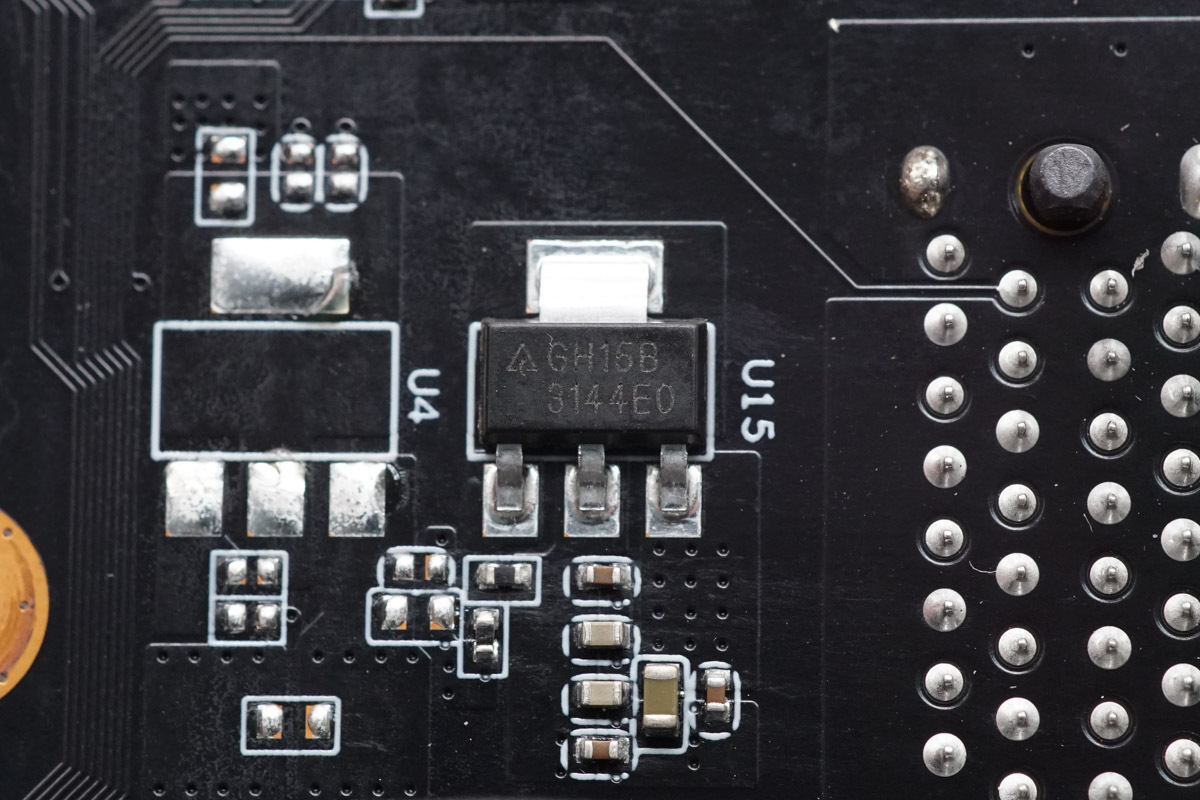
The voltage regulator is from DIODES, marked GH15B, model AZ1117CH-ADJ. It supports an input voltage of up to 18V, provides an adjustable output voltage, and has a 1.35A output current limit. It is housed in an SOT223 package.
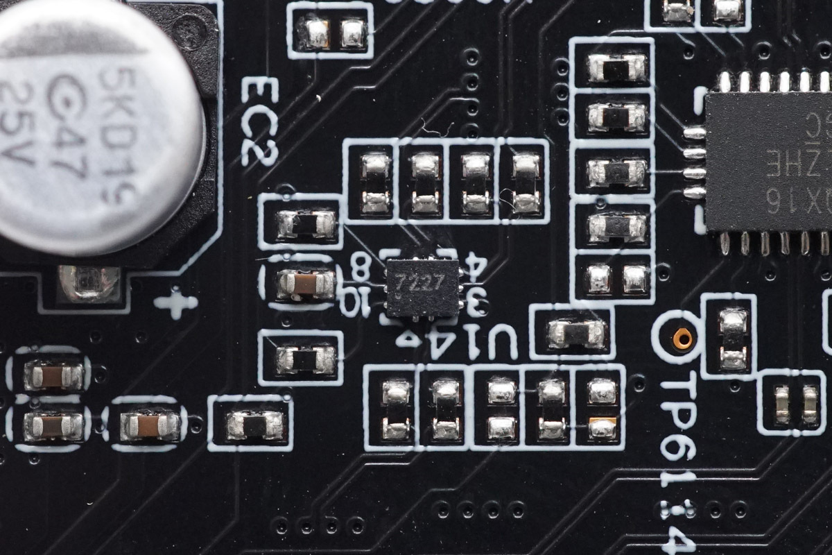
The switching IC, marked 7227.
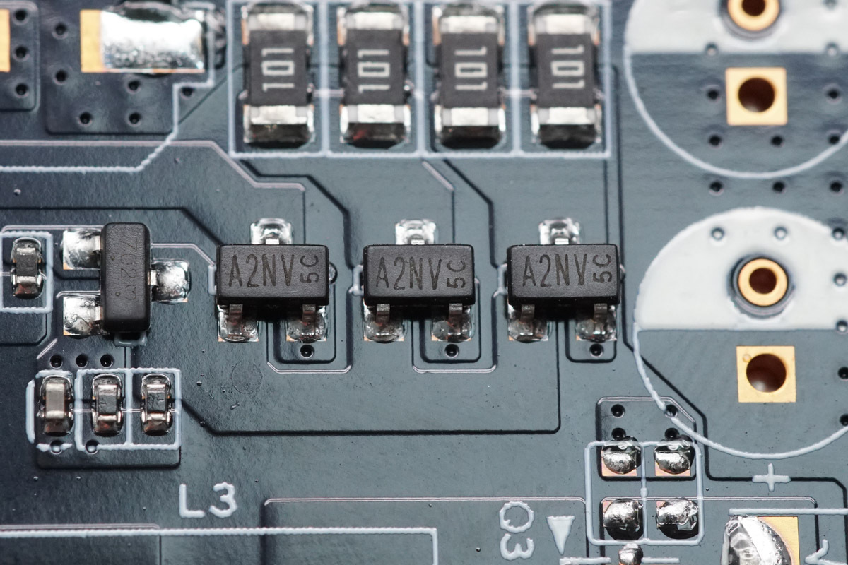
The switching MOSFETs, marked A2NV.
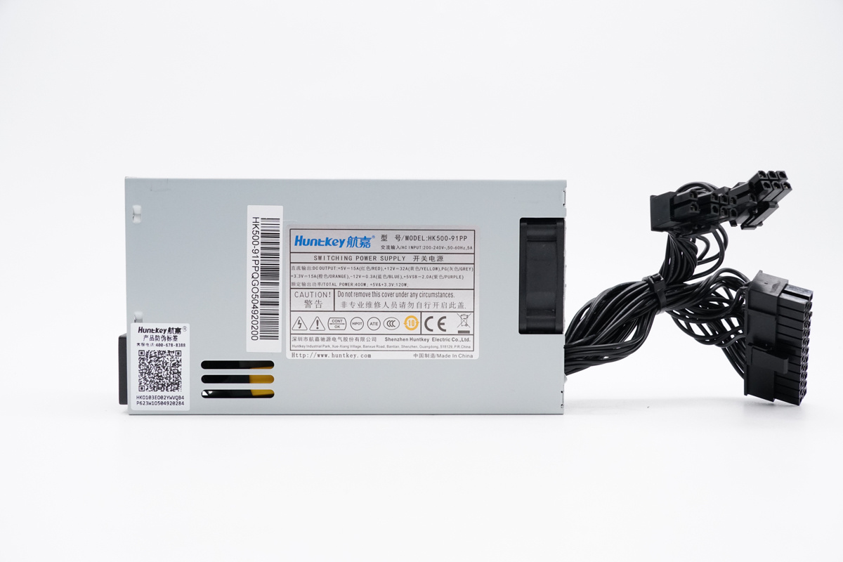
The dock is powered by a built-in Huntkey switching power supply module.
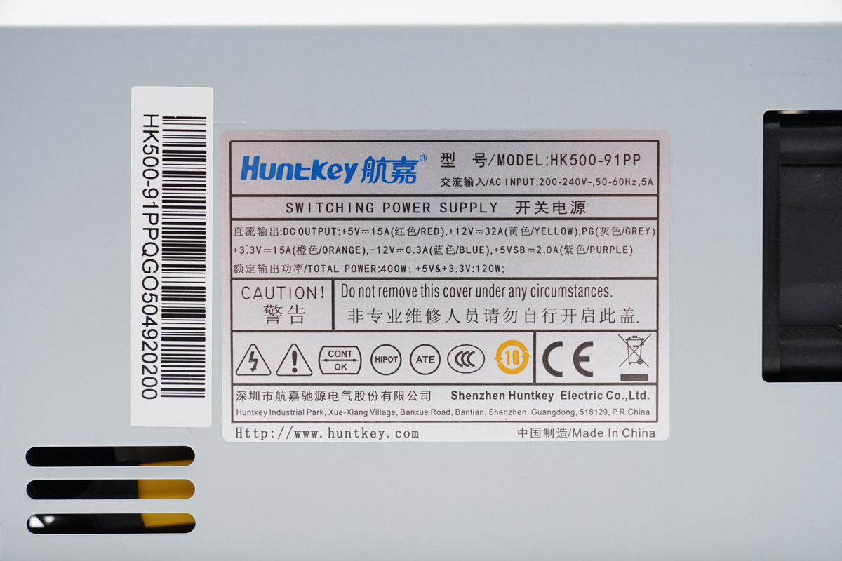
The power supply label:
Model: HK500-91PP
AC Input: 200–240V~, 50–60Hz, 5A
DC Output: +5V ⎓ 15A, +12V ⎓ 32A, +3.3V ⎓ 15A, -12V ⎓ 0.3A, +5VSBV ⎓ 2A
Rated Output Power: 400W
+5V & +3.3V: 120W
The power supply has passed CCC and CE certifications.
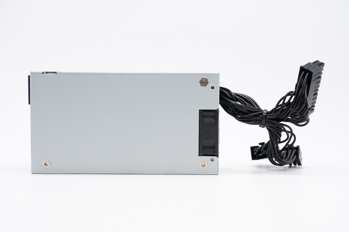
The rear of the enclosure features screw mounting holes.
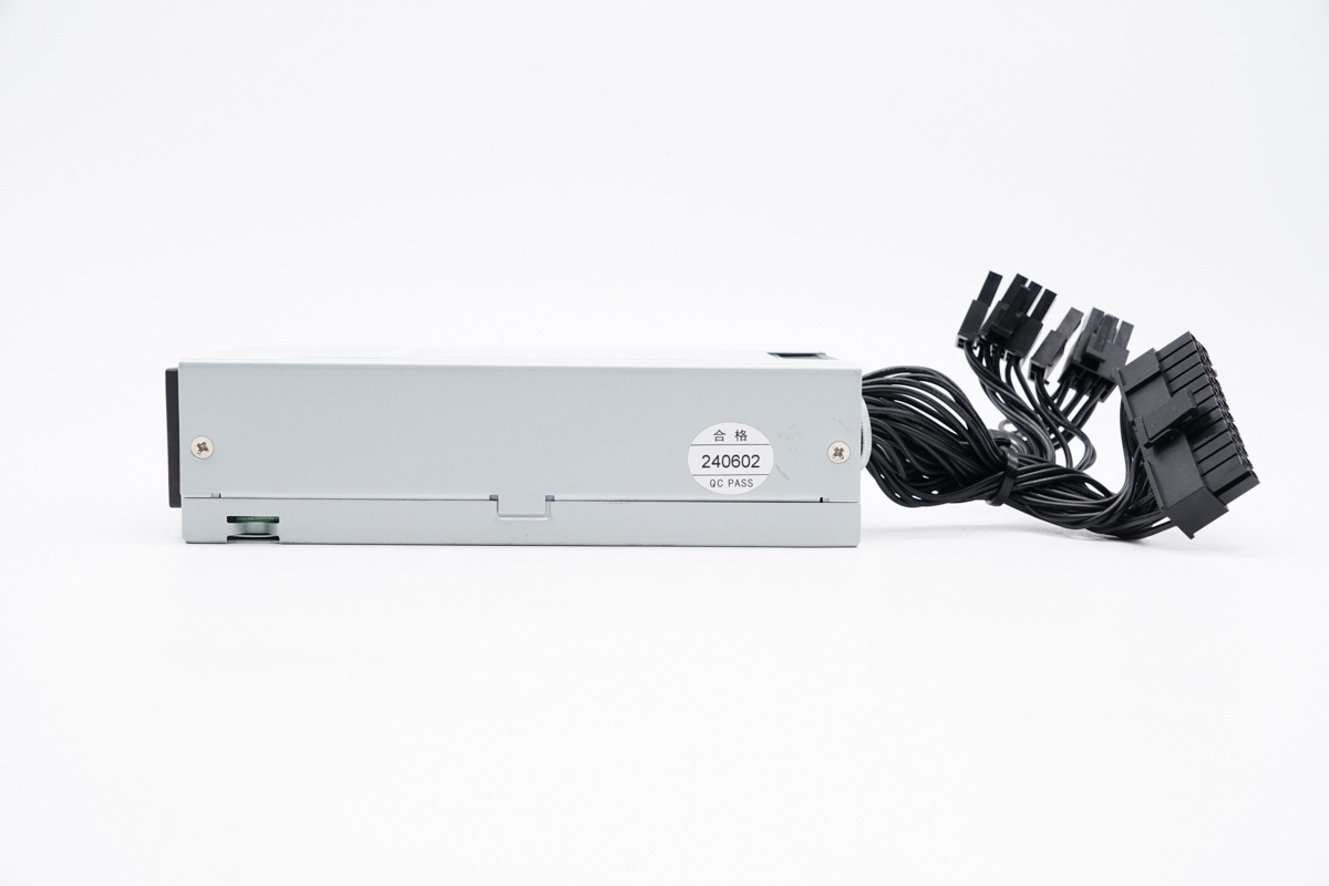
The side is secured with screws and carries a quality inspection label.
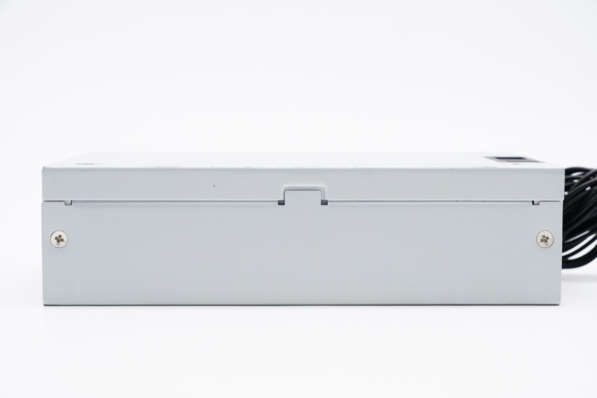
The opposite side also has securing screws.
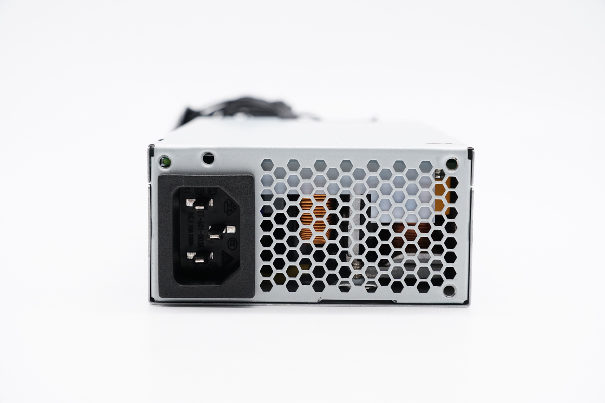
The input end features an AC power inlet and ventilation openings.
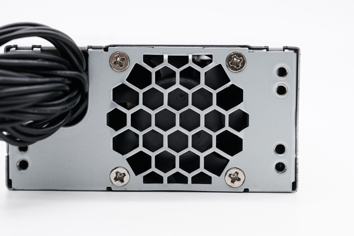
The output end features output cables and a cooling fan.
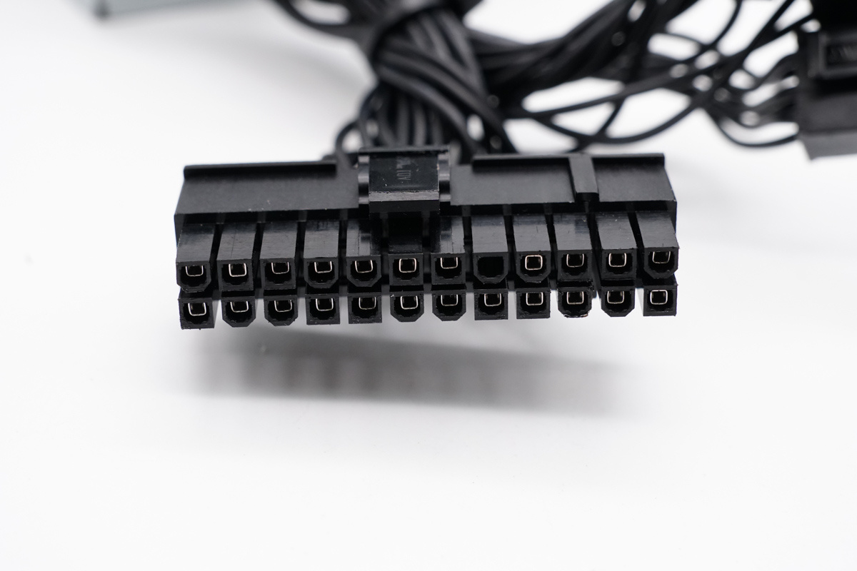
The power supply provides a 24-pin output connector.
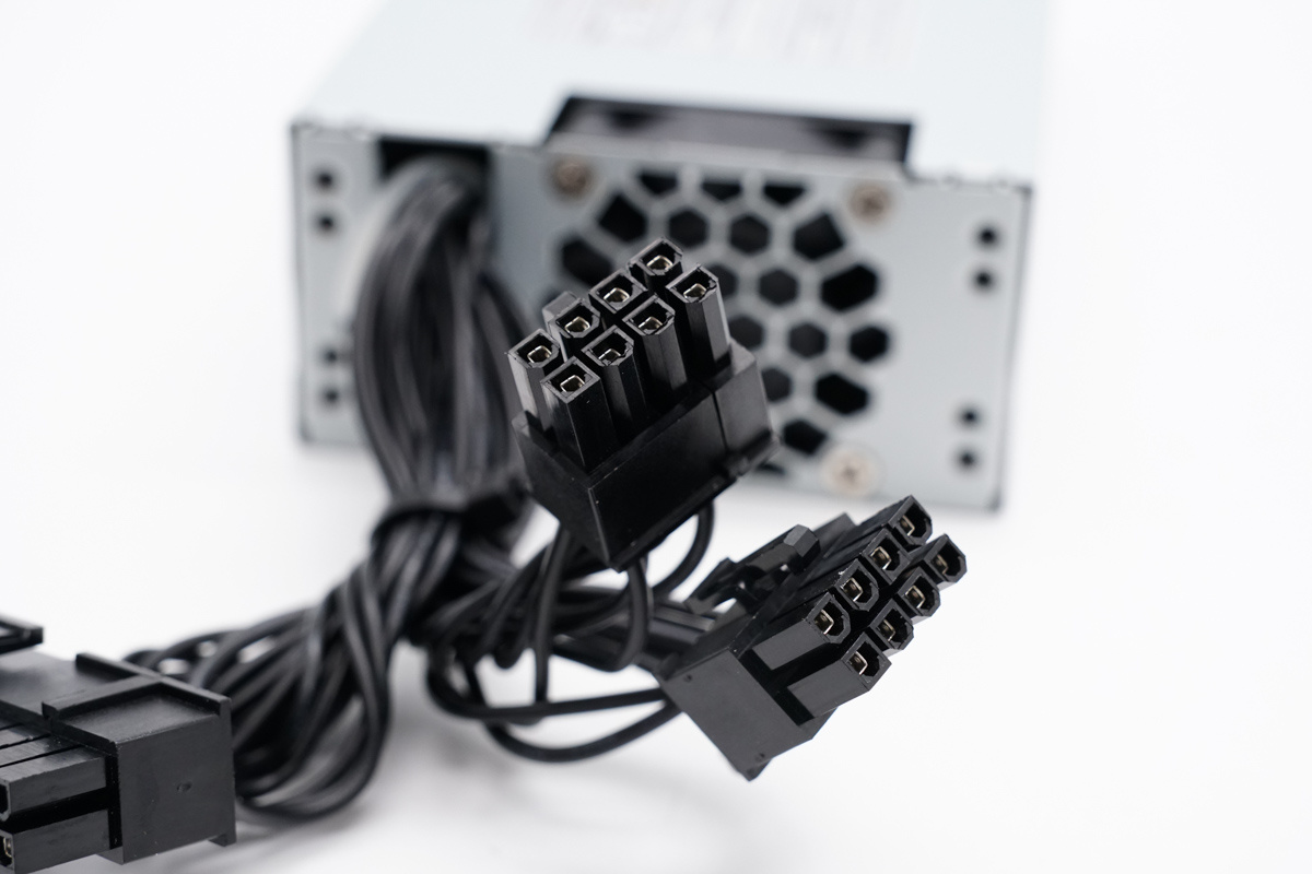
It also provides dual 8-pin output connectors.
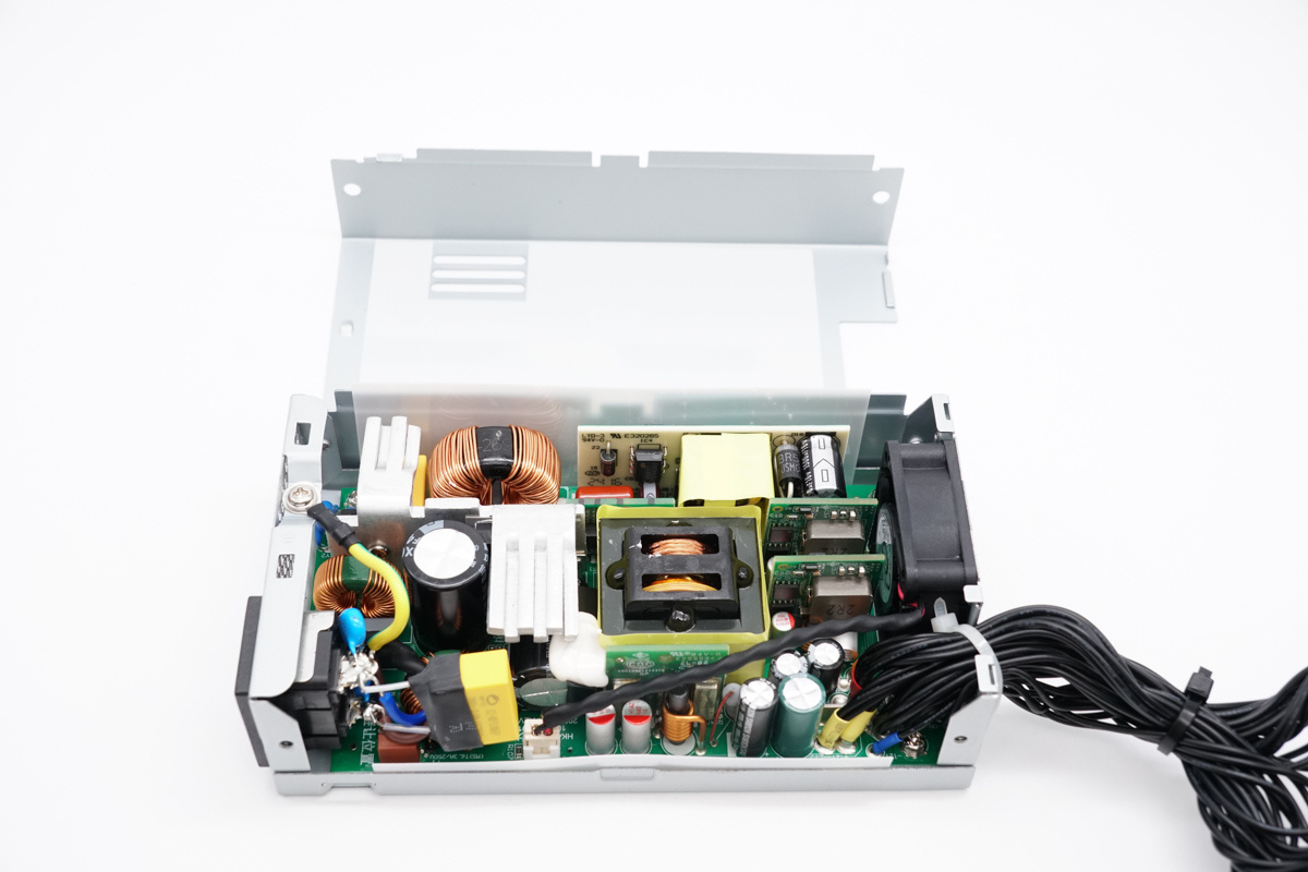
Remove the screws to open the power supply module.
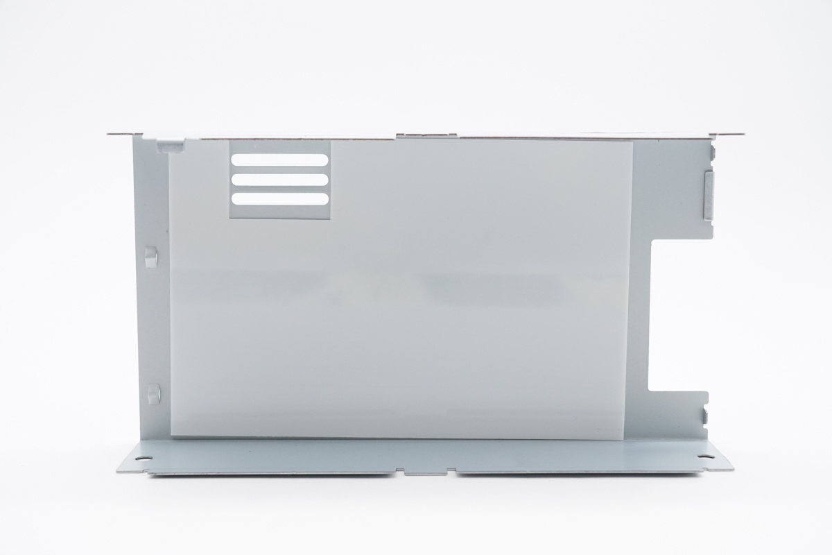
A Mylar insulation sheet is attached inside the top cover.
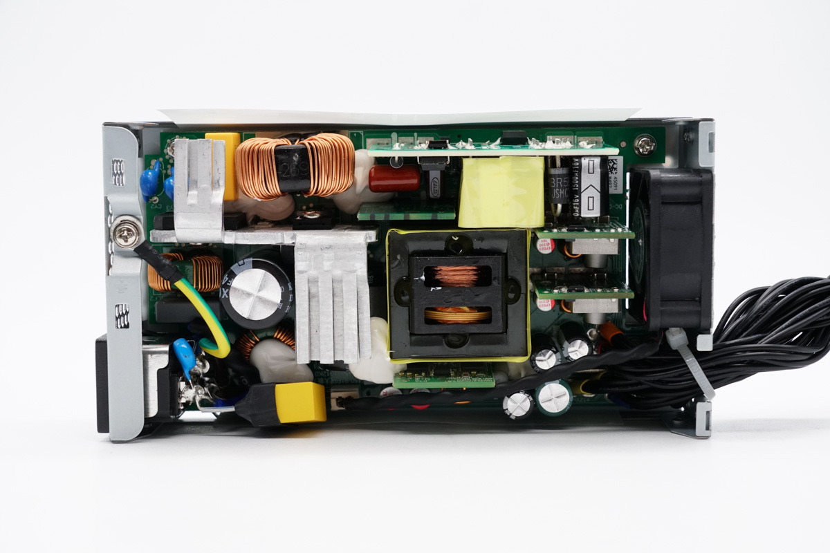
The PCBA module is secured inside the enclosure with screws.
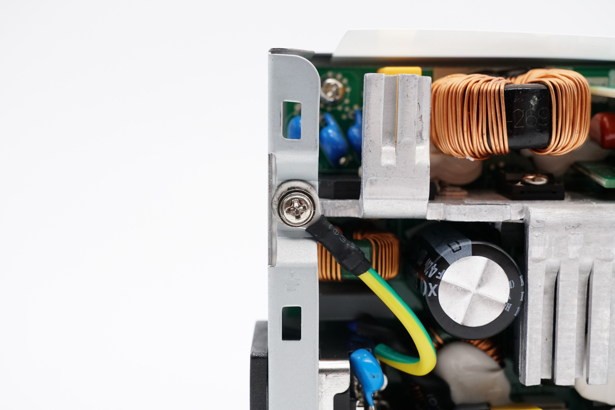
The ground wire is secured to the enclosure with a screw.
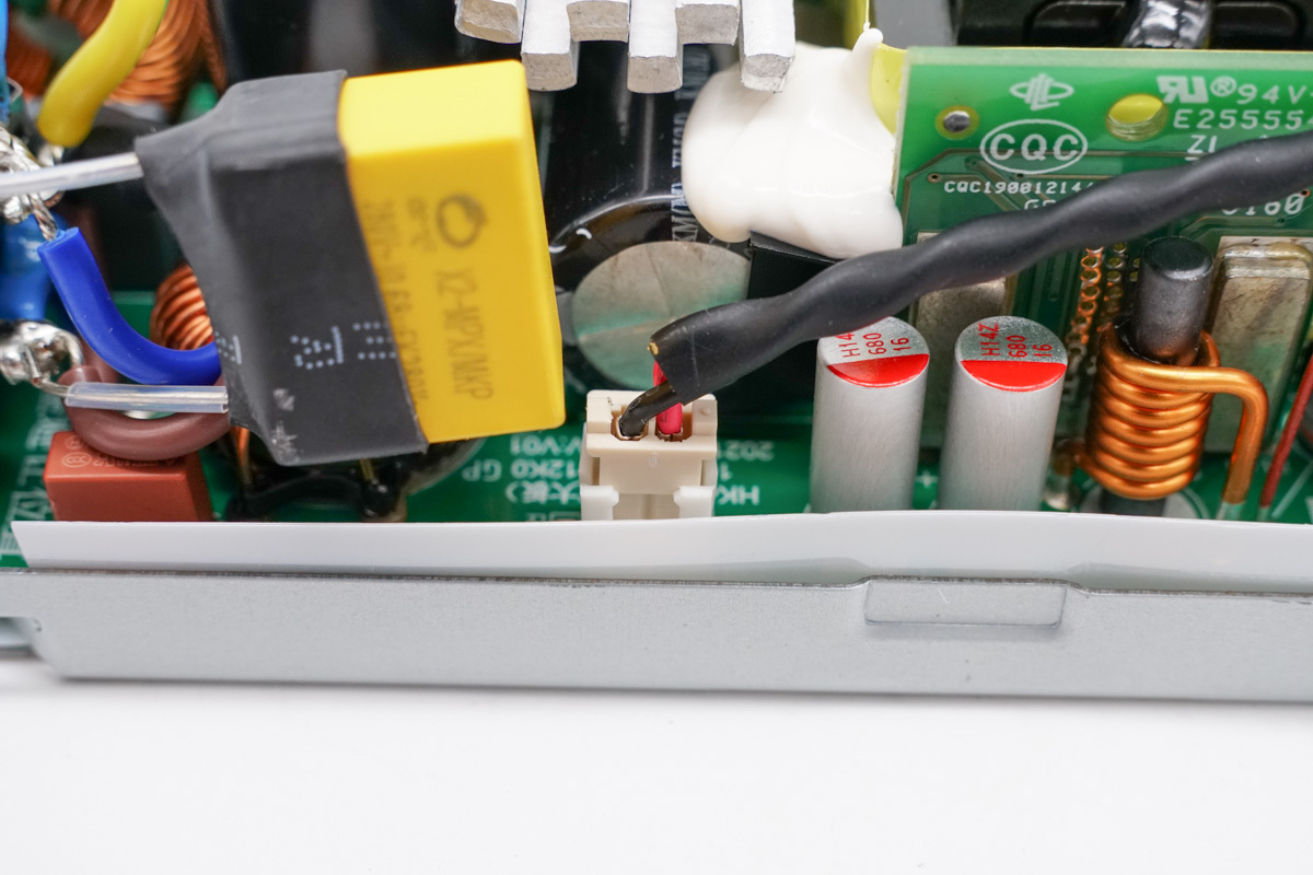
The cooling fan is connected through a connector.
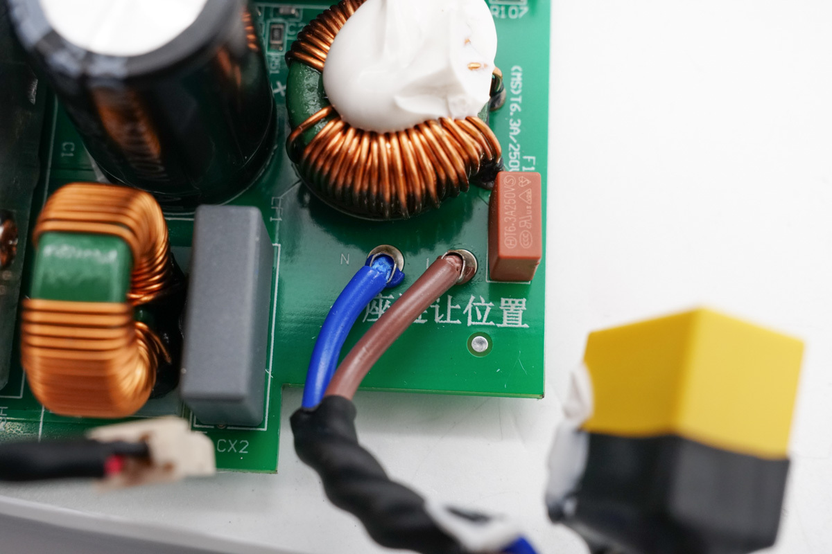
The power input wires are connected by soldering.
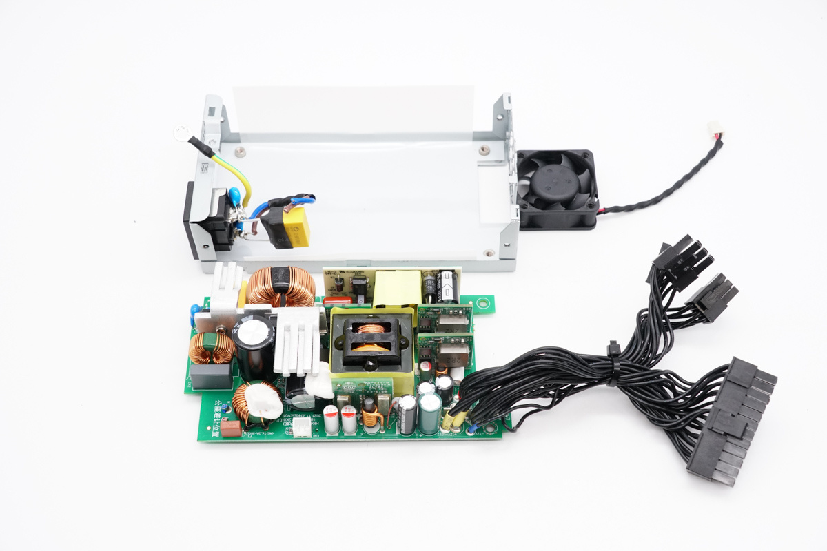
Cut the input wires and remove the PCBA module.
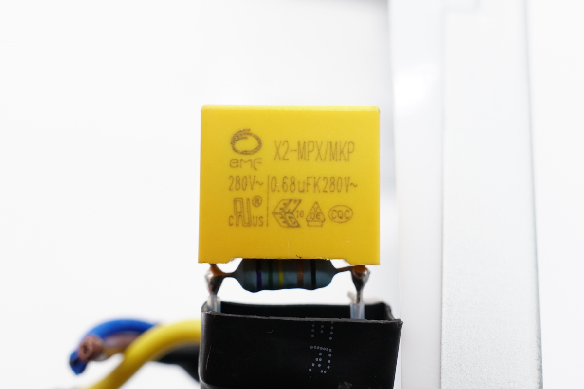
A safety X2 cap is soldered to the AC power inlet, which is from EMF and rated at 0.68μF.
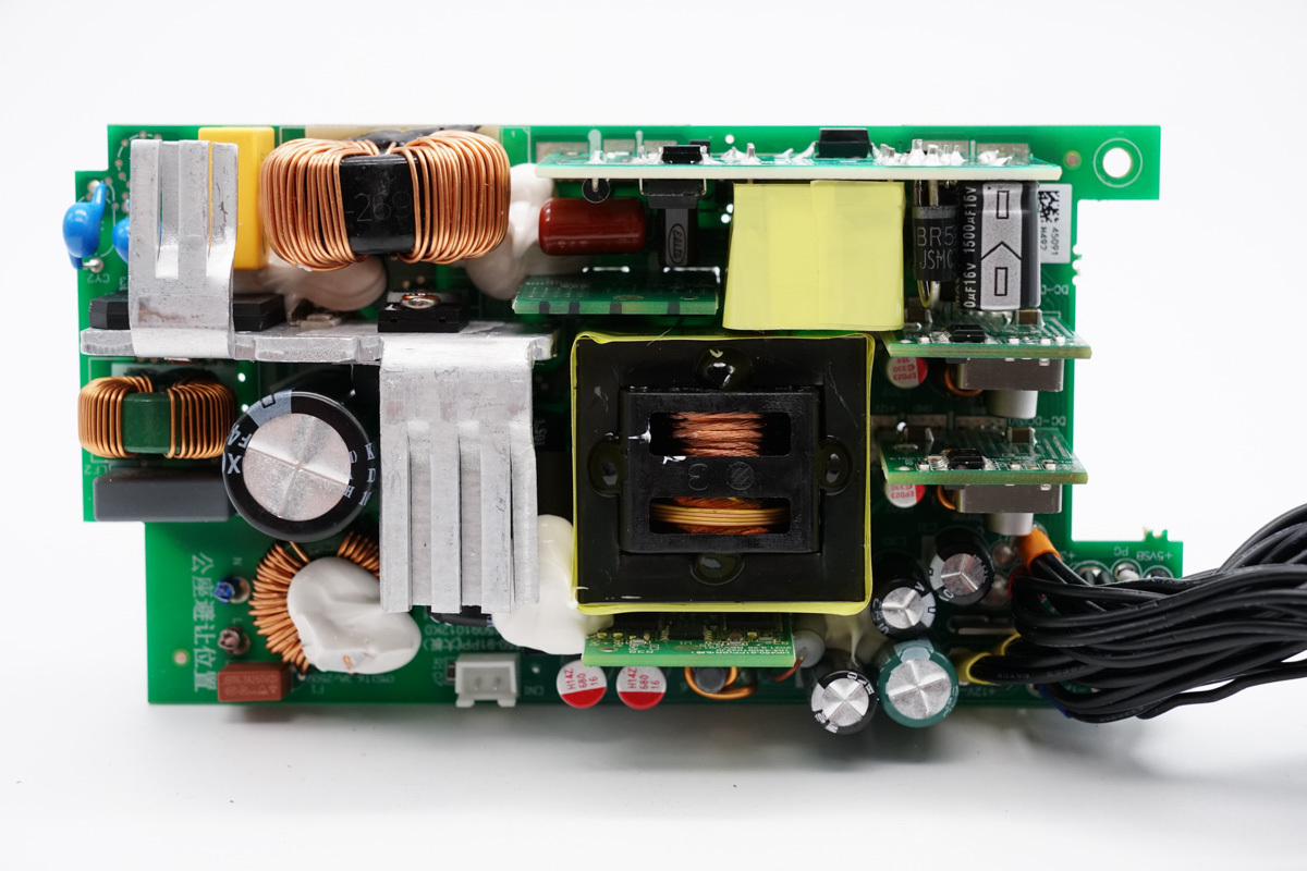
The front of the PCBA module: the lower left section features the fuse, common-mode choke, safety X2 cap, and high-voltage filter caps. The upper section features the bridge rectifier, PFC switching MOSFET, and PFC rectifier MOSFET, along with the PFC boost inductor. The right side features the standby power supply PCB and LLC switching MOSFET PCB.
A synchronous rectification PCB and filter caps are located beneath the LLC transformer. The right side features 3.3V and 5V buck converter PCBs, along with filter caps and soldered output wires.
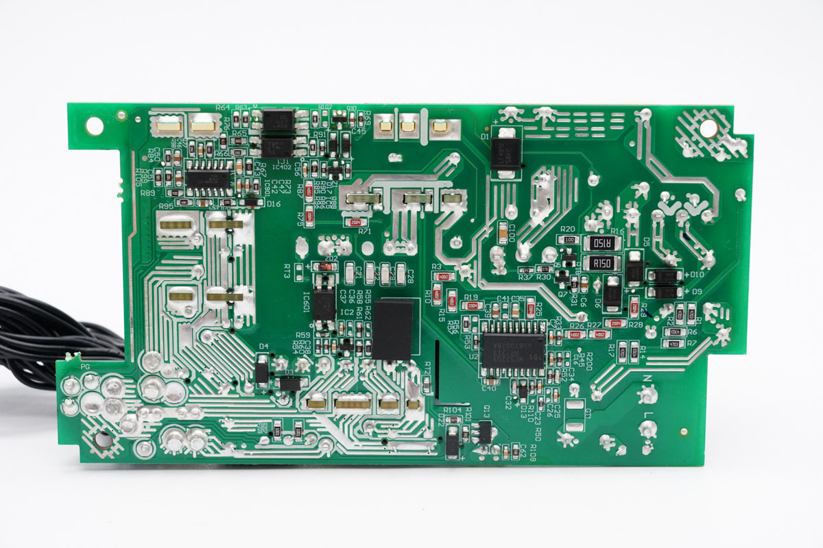
The back side features a two-in-one controller, bypass diode, feedback optocoupler, and control IC.
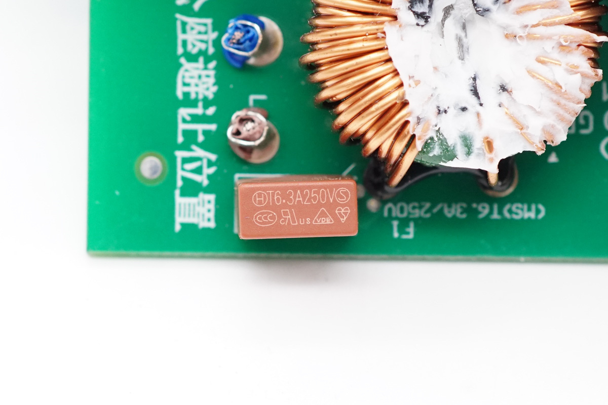
The input fuse is rated at T6.3A 250V.
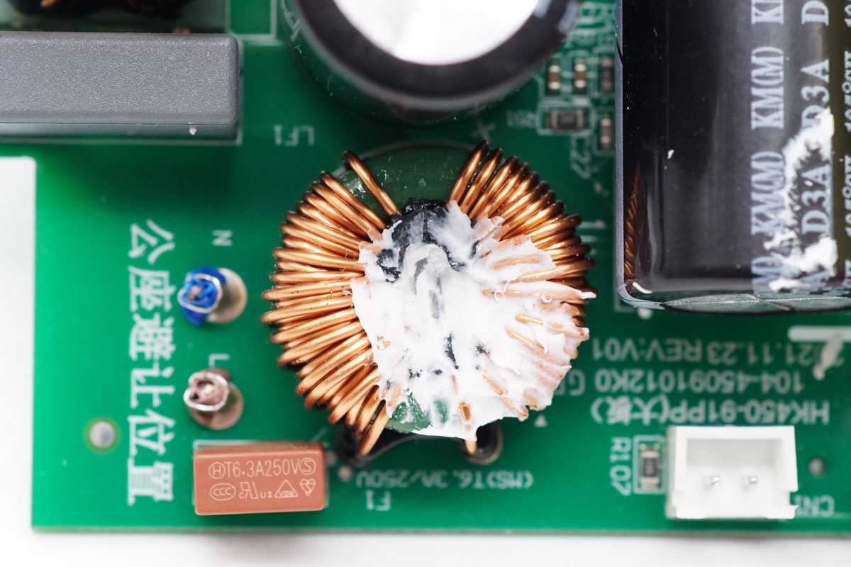
The common-mode choke is wound with enameled wire and insulated from the bottom by a bakelite board.
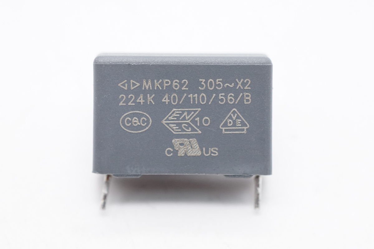
The safety X2 cap is from Faratronic, and rated at 0.22μF.
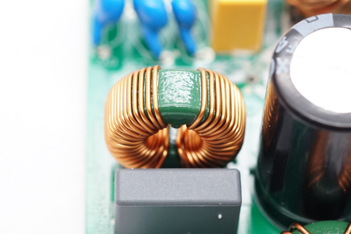
The other common-mode choke.
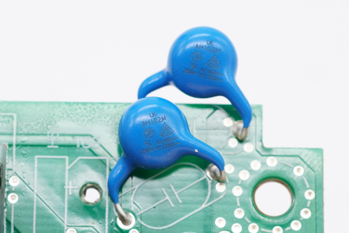
The blue Y-cap is from WTC and marked AH102M.
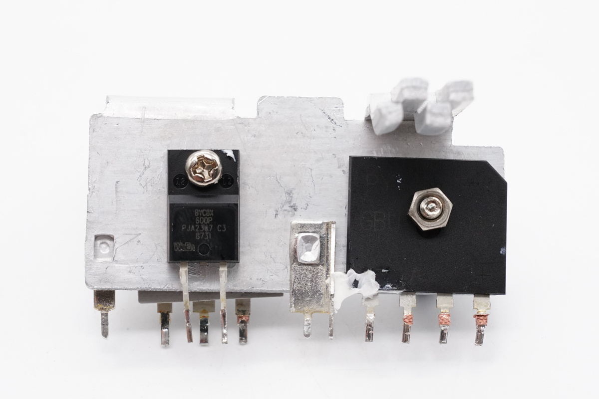
The heatsink is equipped with the bridge rectifier and PFC rectifier MOSFET.
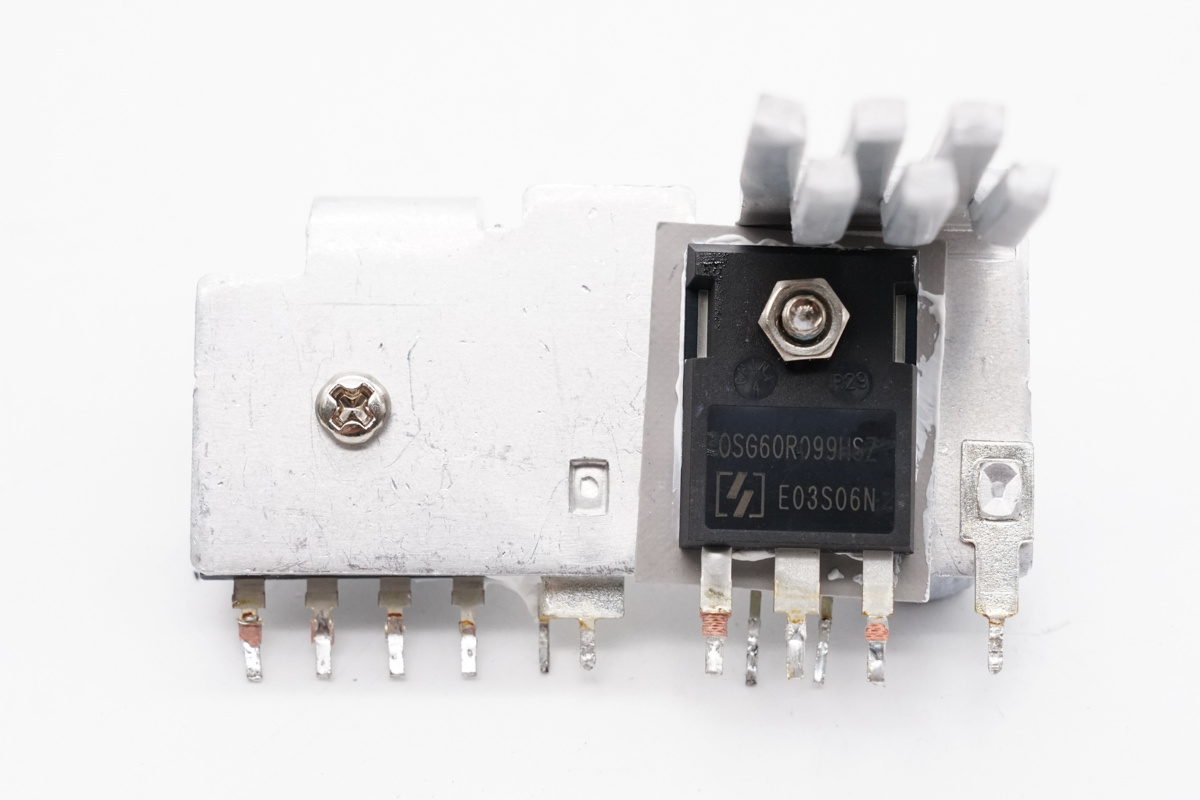
The PFC switching MOSFET is installed on the opposite side.
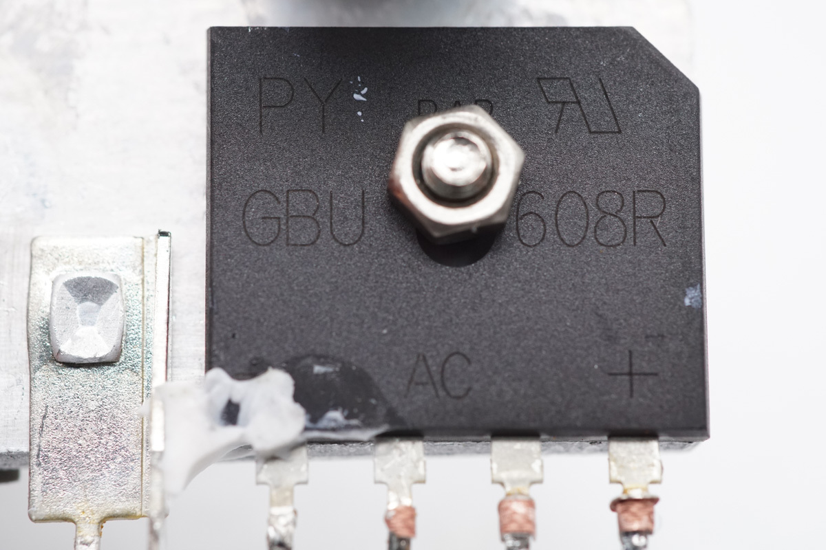
The bridge rectifier is from PINGWEI, model GBU608R, rated at 800V 6A, and housed in a GBU package.
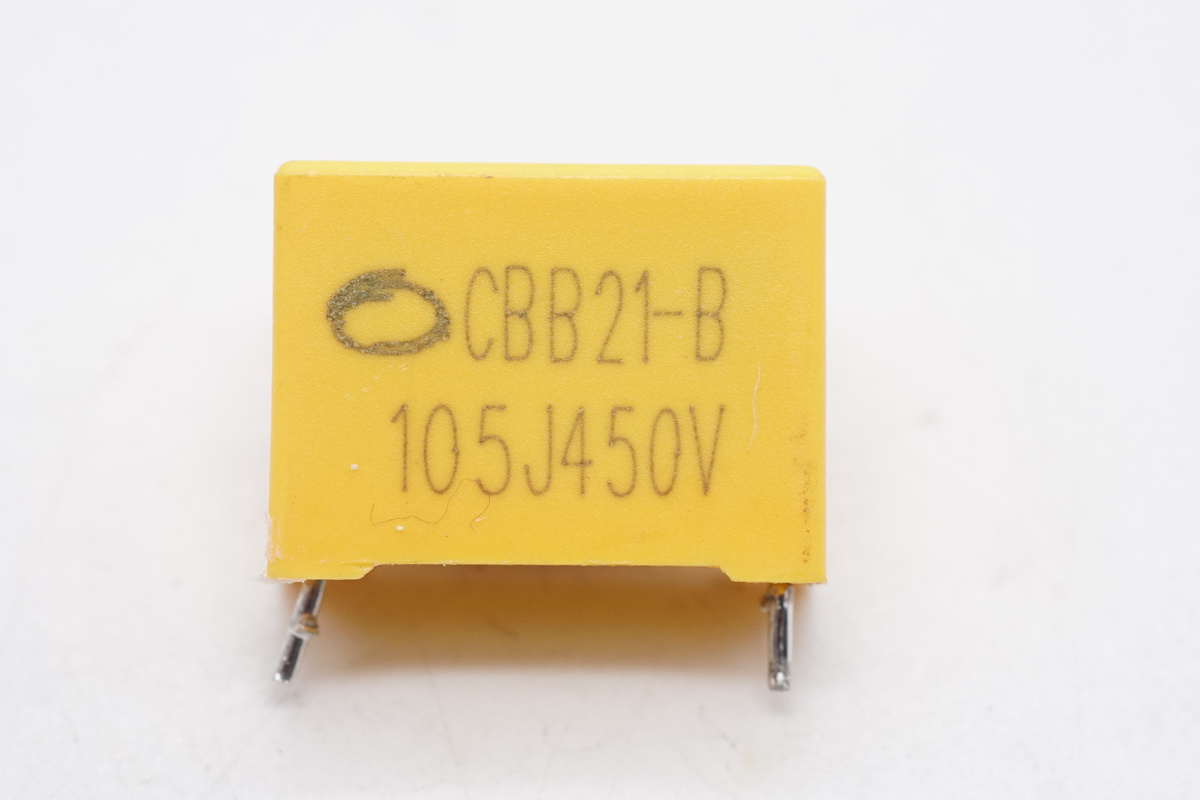
The film filter cap is from EMF and rated at 1μF 450V.
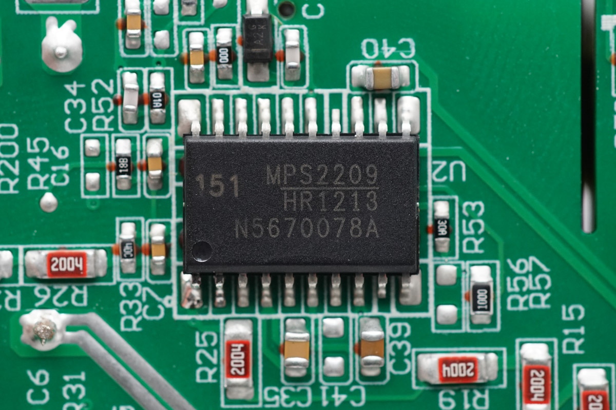
The two-in-one controller is from MPS, model HR1213. It is a multi-mode PFC and current-mode LLC combination controller that supports both AC and DC input, with configurable bias options. The PFC controller supports mixed CCM and DCM operation and burst mode.
The LLC stage supports steady-state, skip, and burst modes, along with adaptive dead-time adjustment and capacitive-mode protection. The chip integrates high-voltage startup, thermal shutdown, PFC switch protection, OVP, overcurrent limiting, LLC OCP, and OCP. It also provides a UART configuration interface and is housed in an SOIC-20 package.
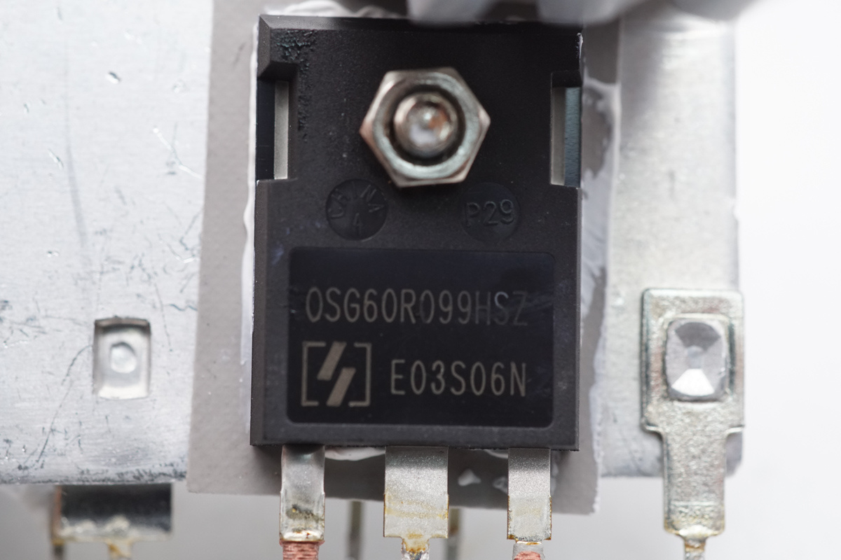
The PFC switching MOSFET is from Oriental, model OSG60R099HSZF-F, NMOS, 600V and 99mΩ, and is housed in a TO-247 package.
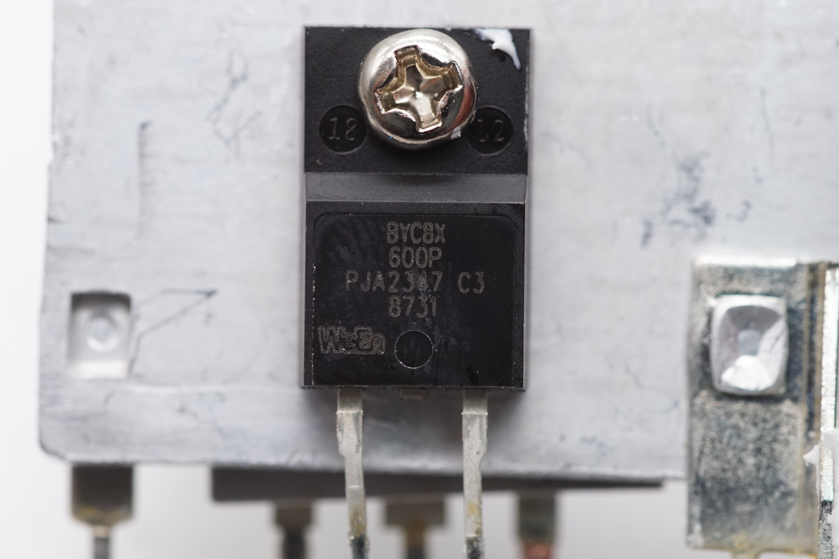
The PFC rectifier diode is from WeEn, model BYC8X-600P. It is an ultrafast diode rated at 600V 8A and housed in a TO-220F package.
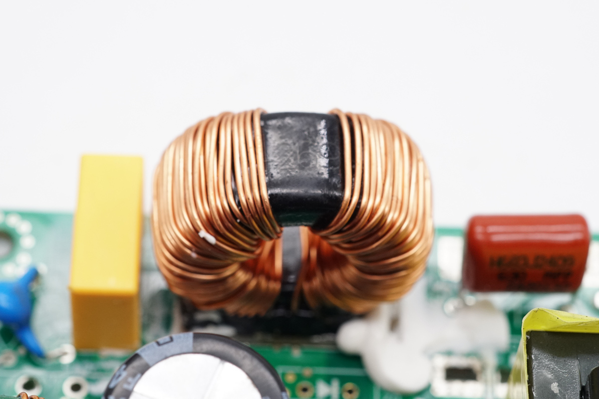
The PFC boost inductor is wound with enameled wire and insulated from the bottom by a bakelite board.
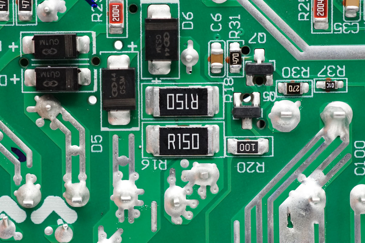
Two 150mΩ resistors are connected in parallel for MOSFET current sensing.
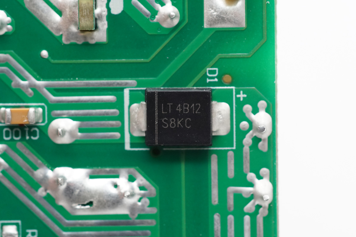
The bypass diode is from DIODES, model S8KC, rated at 800V 8A and housed in an SMC package.
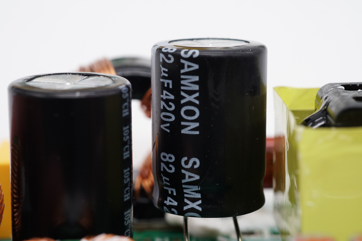
The high-voltage filter cap is from SAMXON and rated at 82μF 420V.
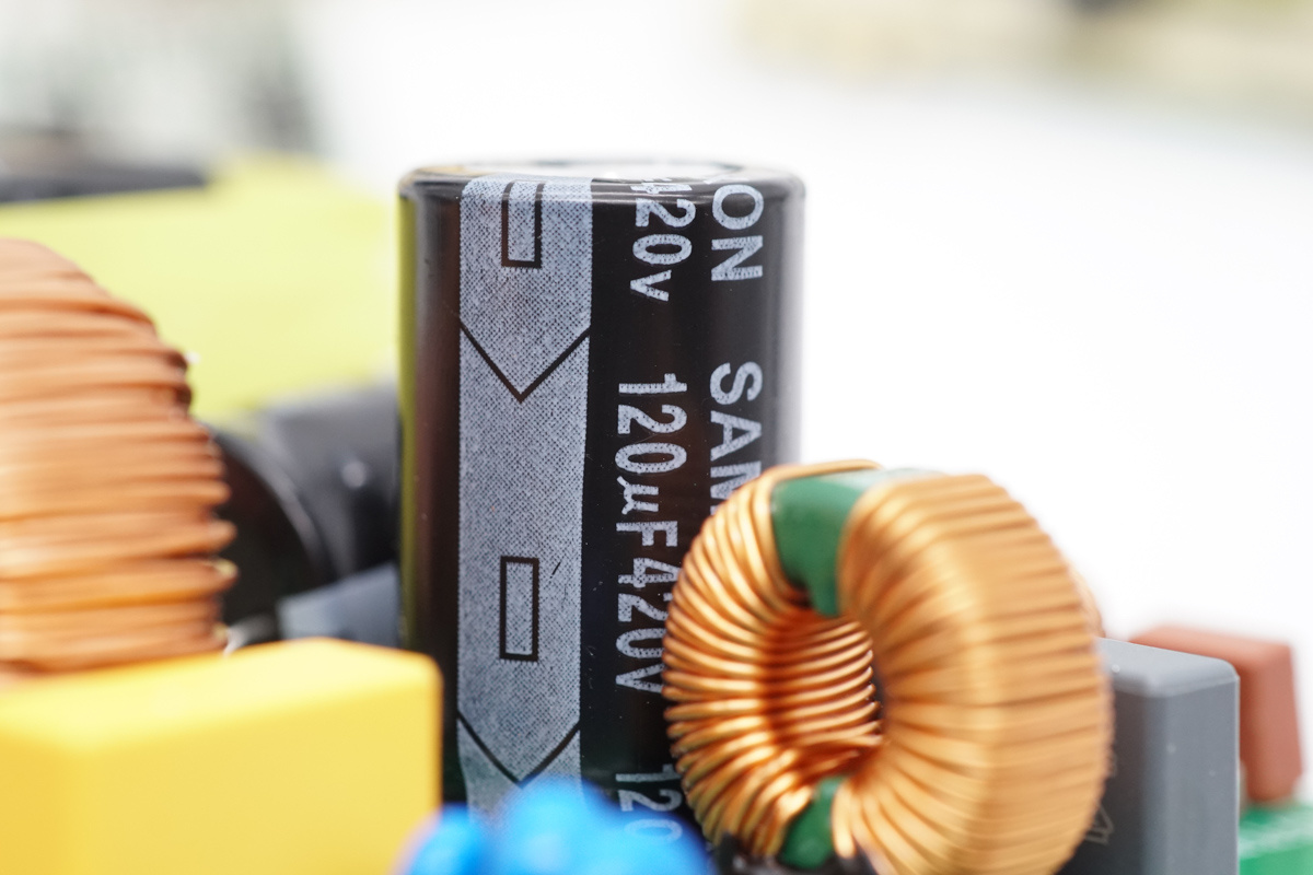
The other one is rated at 120μF 420V.
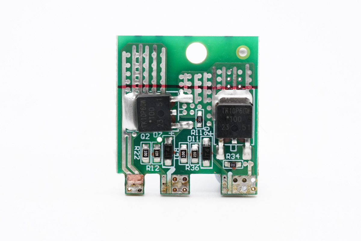
The LLC switching MOSFETs are soldered onto a vertical PCB.
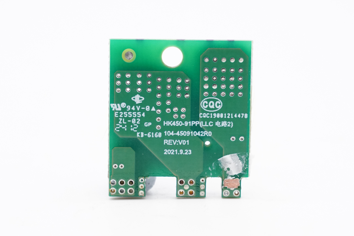
The back of the PCB is free of components and features a large copper area for heat dissipation.
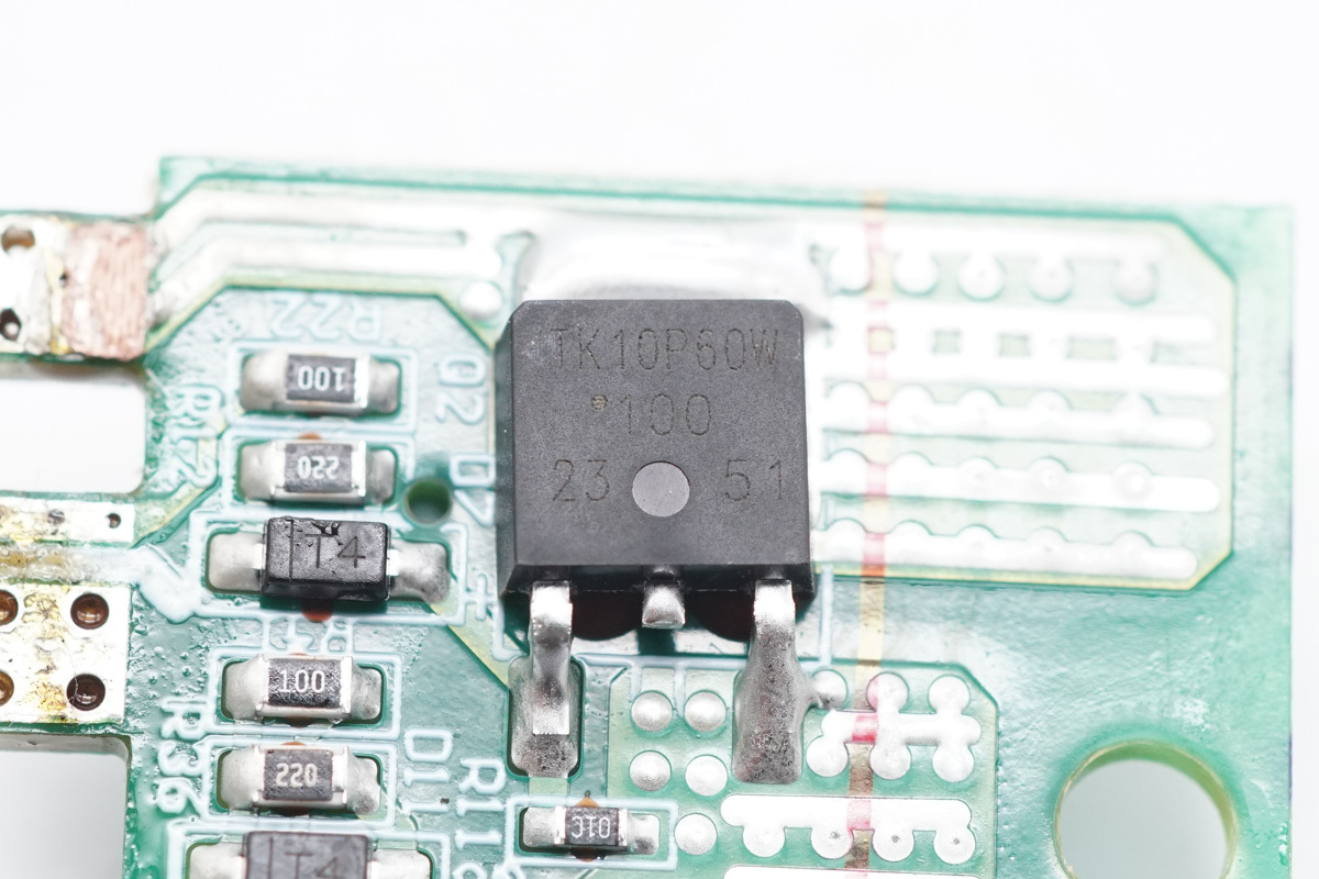
The LLC switching MOSFET is from TOSHIBA, model TK10P60W, NMOS, 600V and 327mΩ, and is housed in a DPAK package.
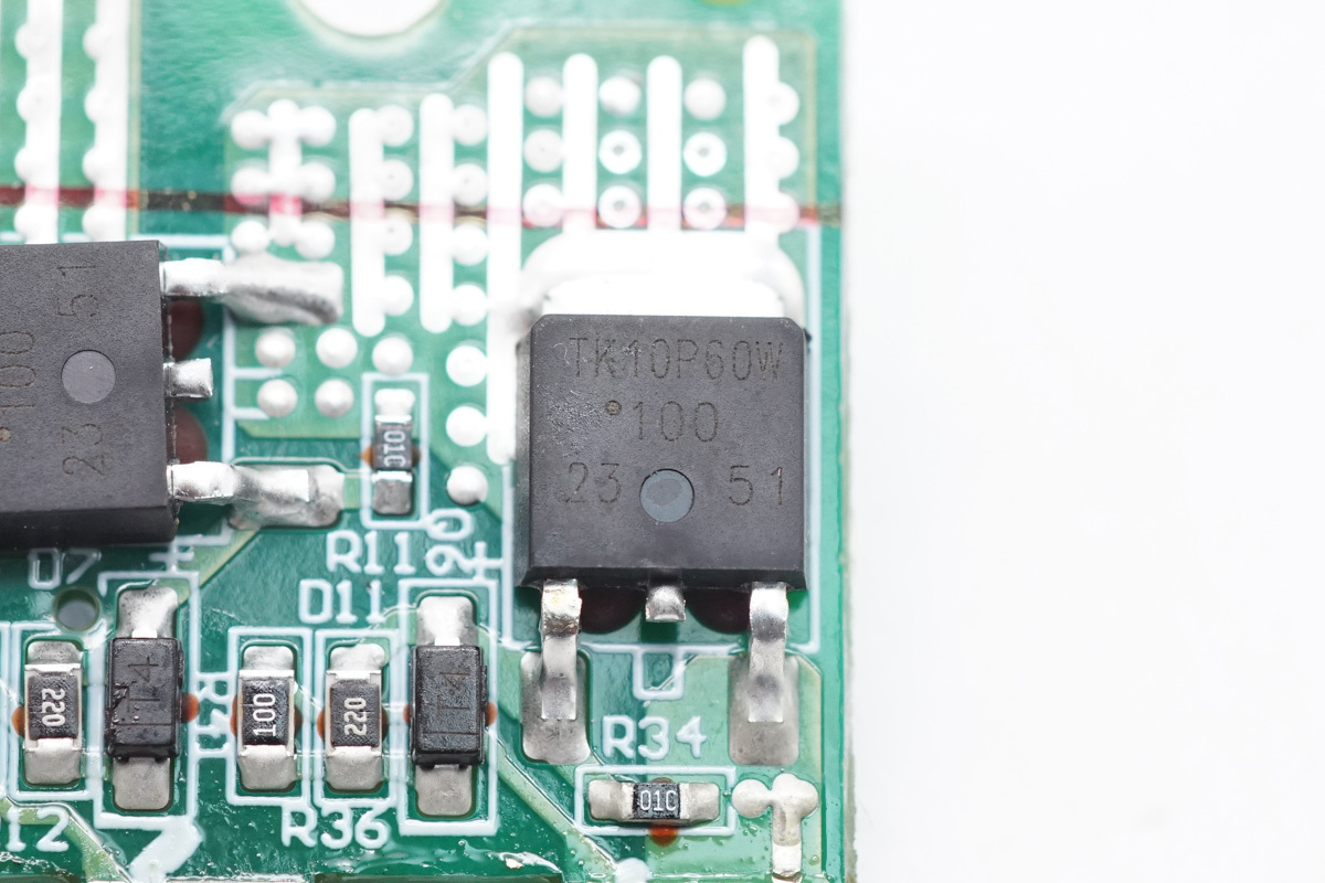
The other one shares the same model.
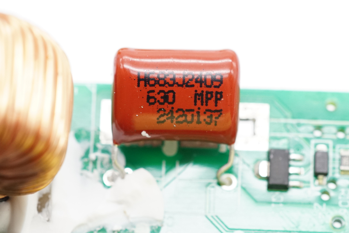
The resonant cap is rated at 0.068μF 630V.
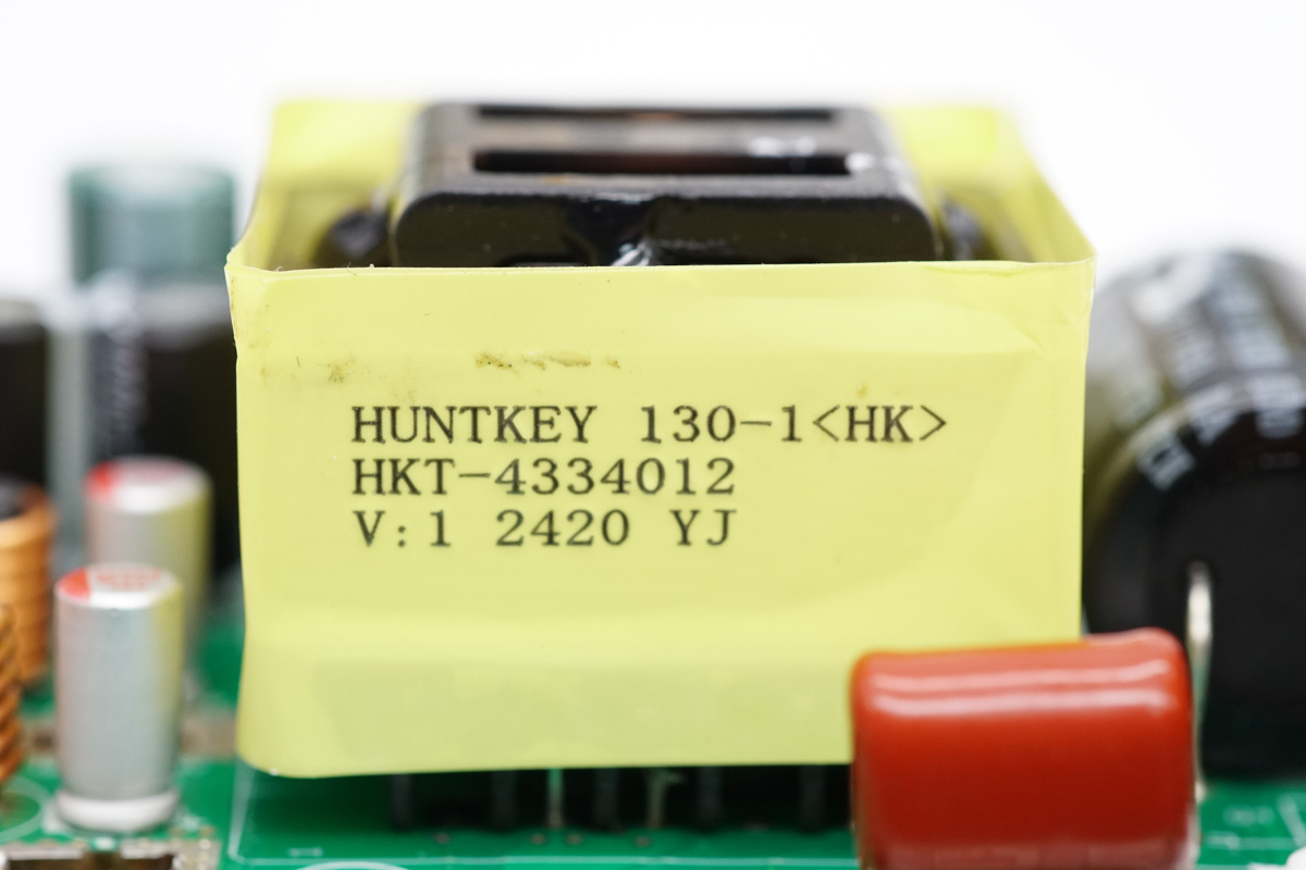
The transformer core is wrapped with insulating tape.
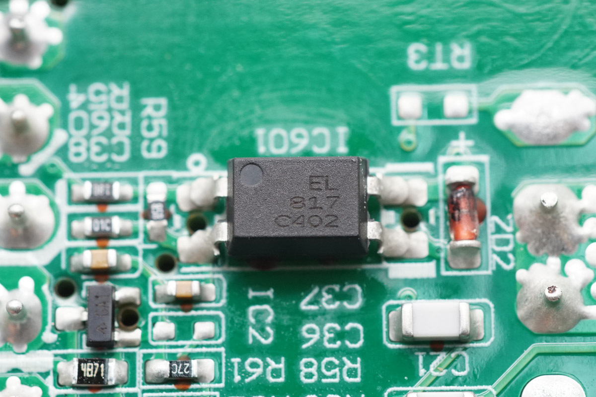
An Everlight EL817 optocoupler is used for output voltage feedback.
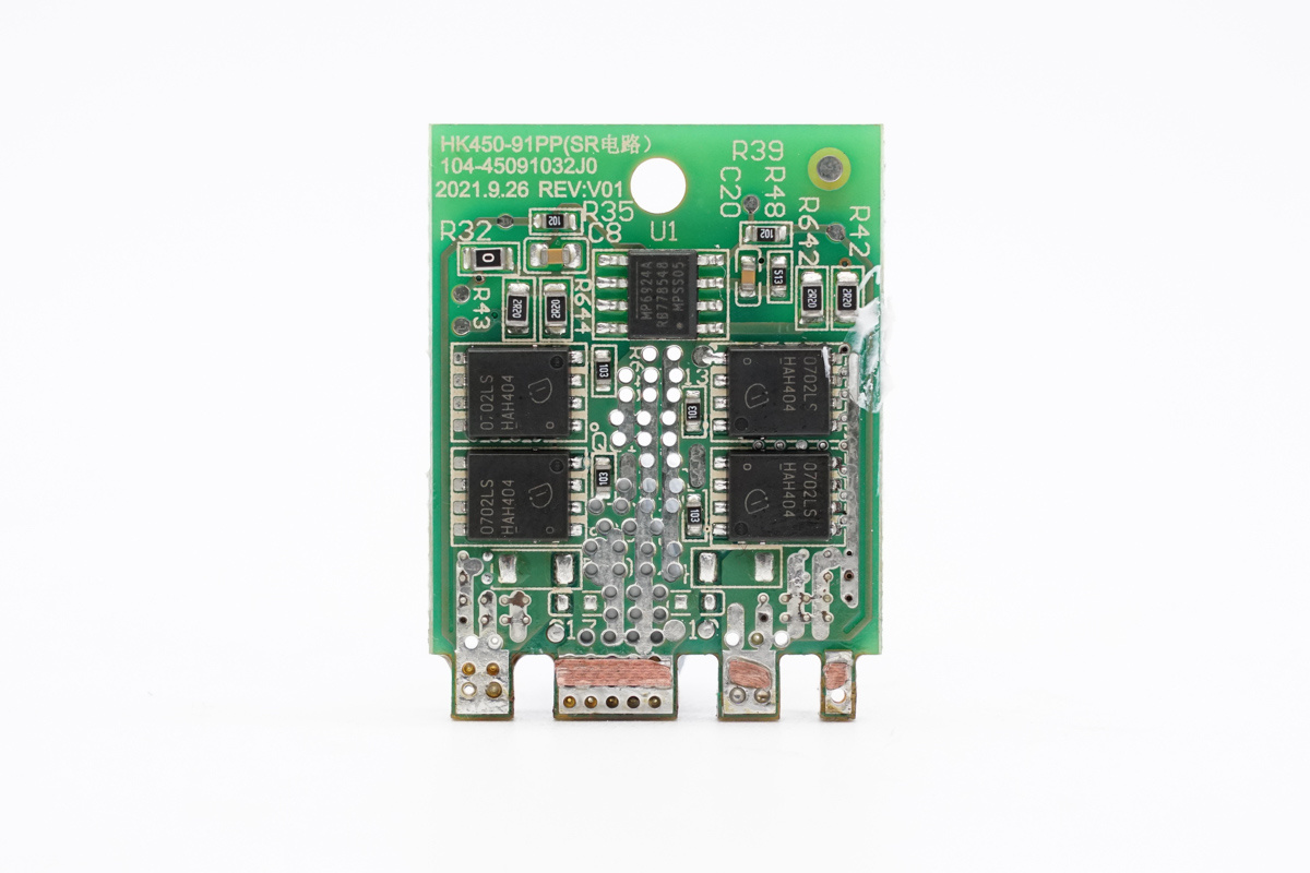
The synchronous rectification controller and synchronous rectifier MOSFETs are soldered onto a vertical PCB.
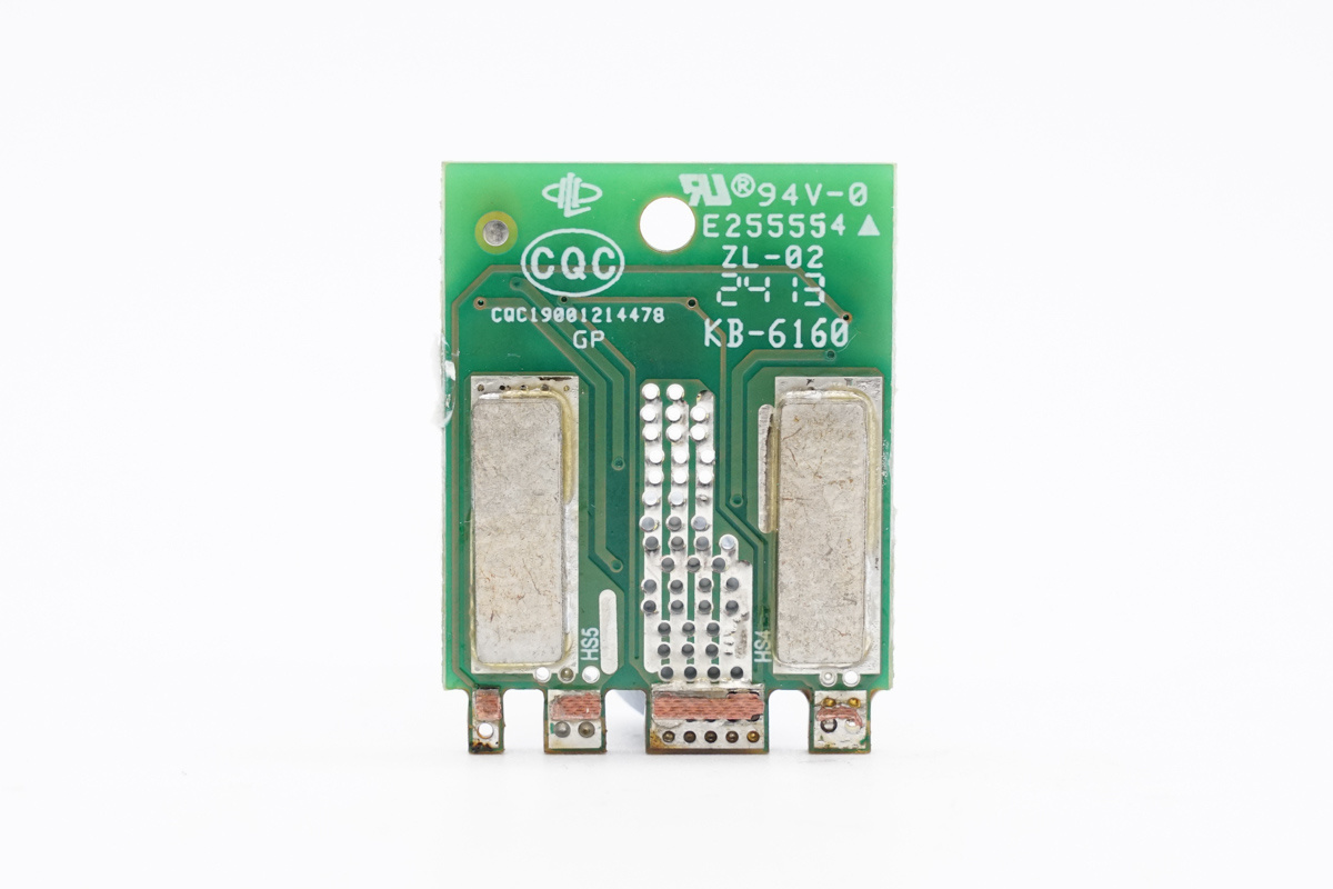
Copper sheets are soldered to the back of the PCB to enhance heat dissipation.
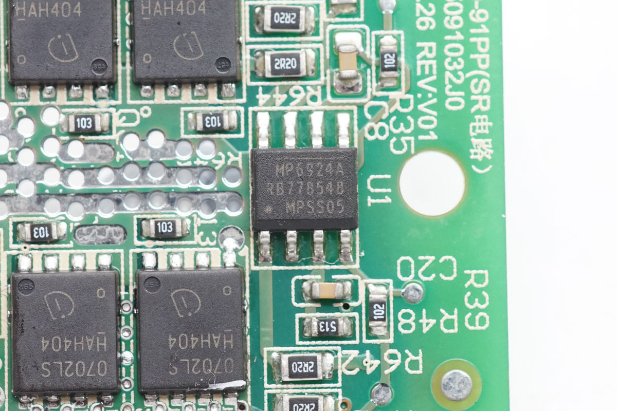
The synchronous rectification controller is from MPS, model MP6924A. It is an LLC synchronous rectification controller featuring enhanced noise immunity and fast turn-off, and is compatible with CCM/DCM operation. The MP6924A integrates two synchronous rectification controllers for rectifying the outputs of the two secondary windings of an LLC transformer. It is designed for synchronous rectification in LLC converters and is housed in an SOIC-8 package.
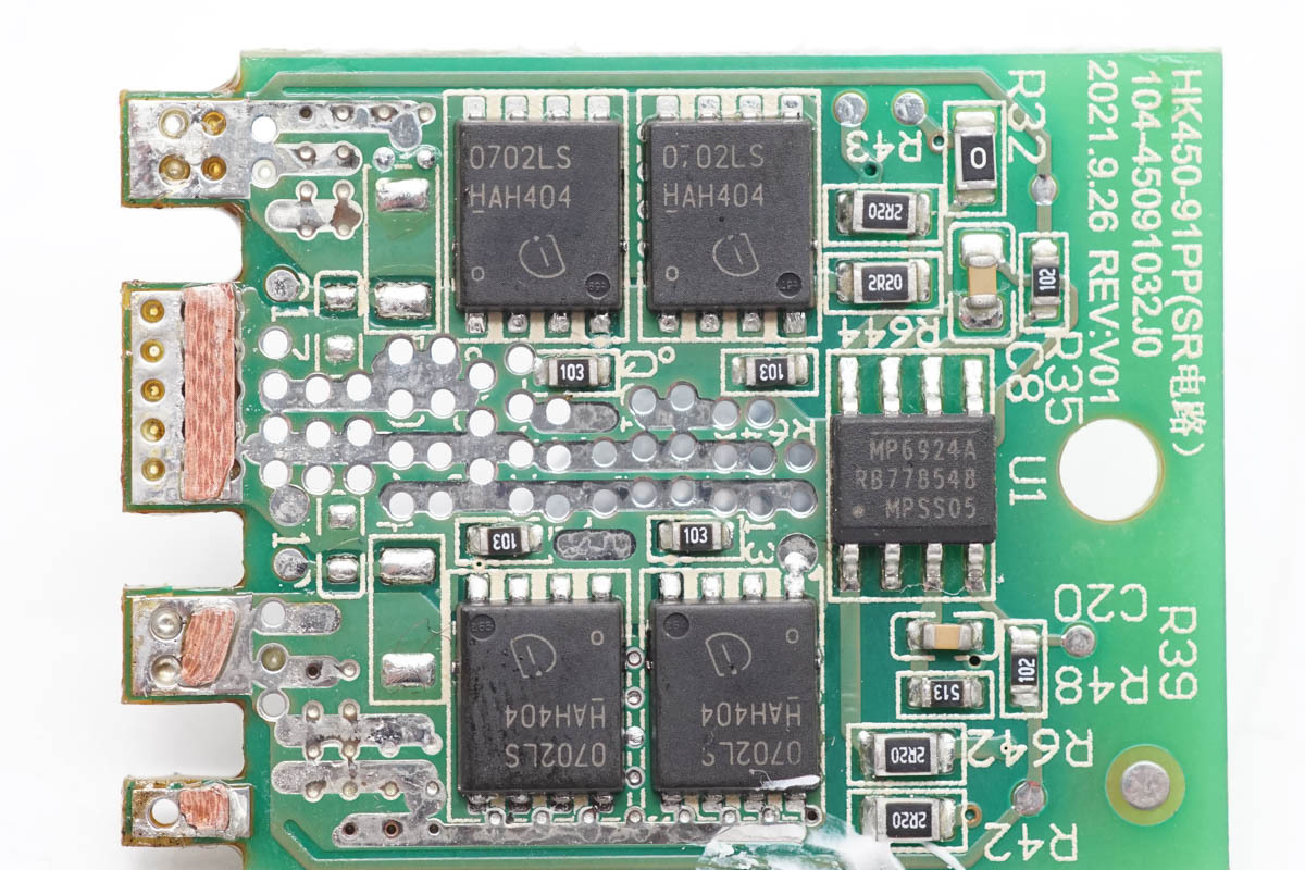
The synchronous rectifier MOSFET is from Infineon, model BSC0702LS, NMOS, 60V and 2.7mΩ, housed in a TDSON-8 package.
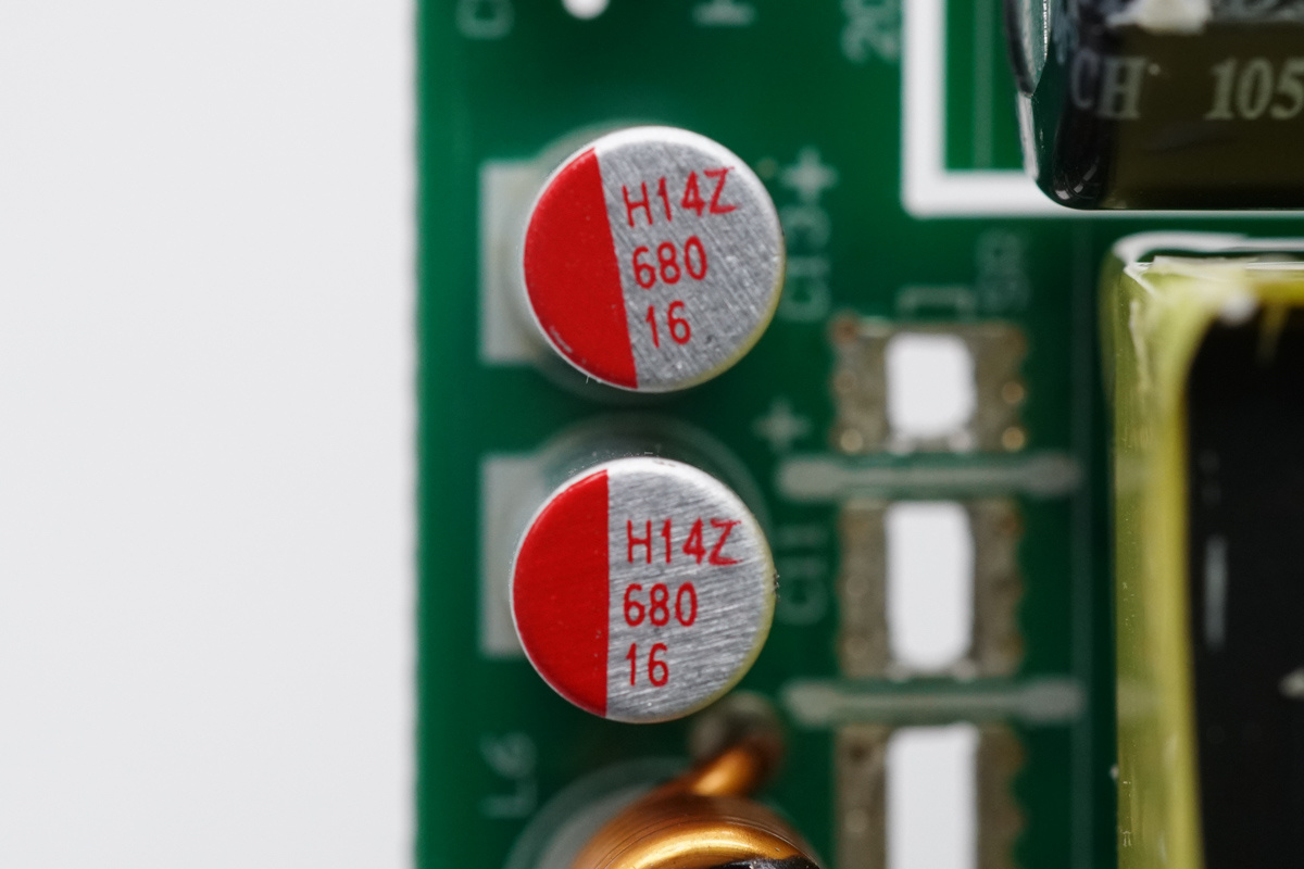
The filter cap is from AiShi and rated at 680μF 16V.
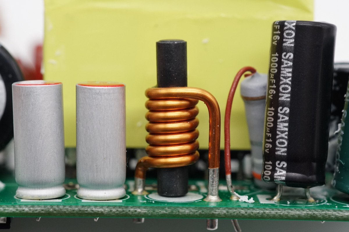
The filter inductor is wound with enameled wire.
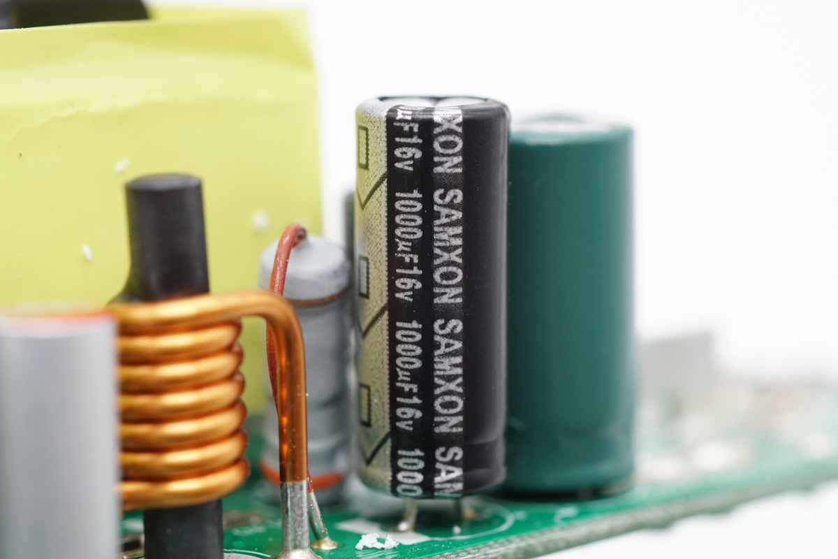
The filter cap is from SAMXON and rated at 1000μF 16V.
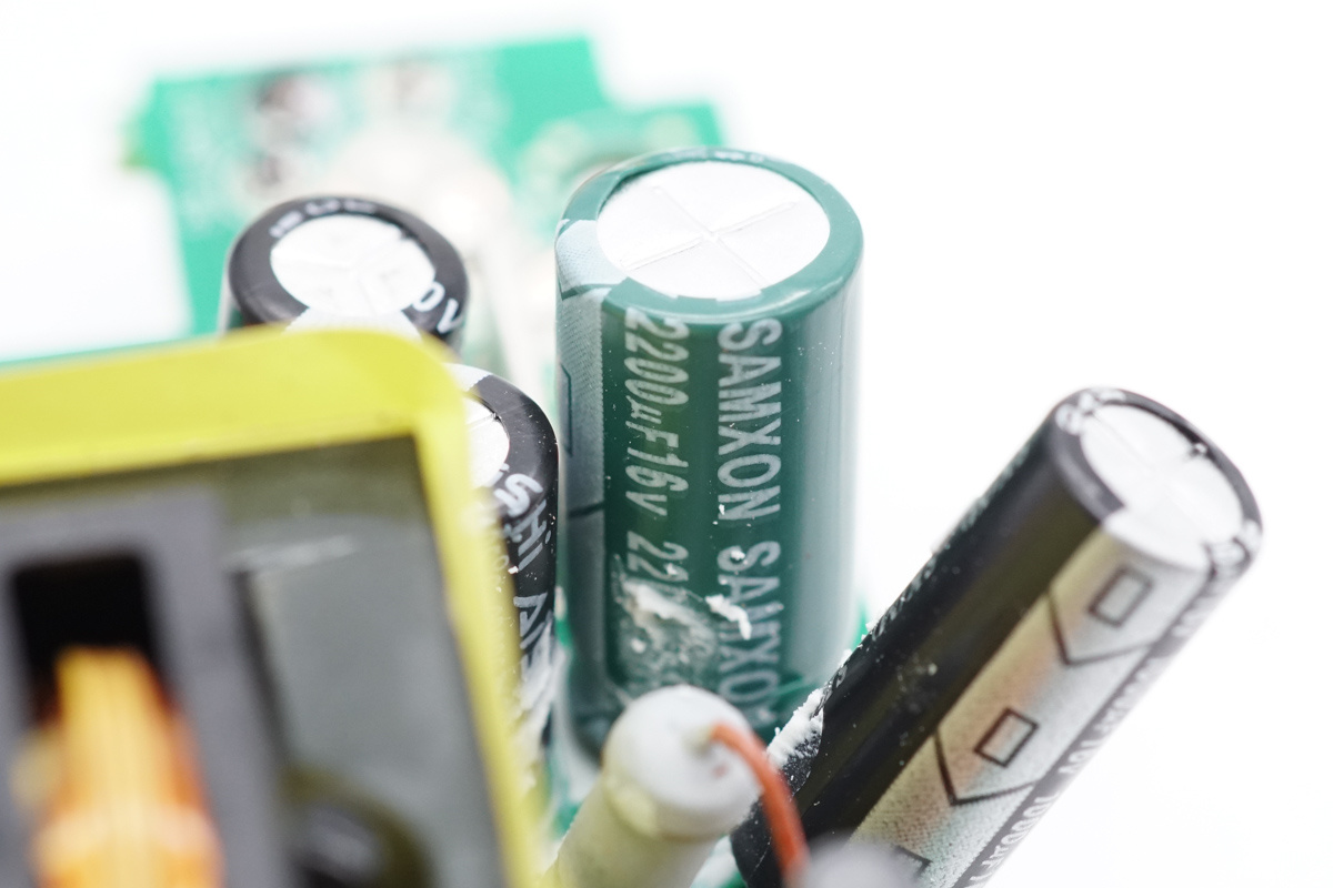
The other one is rated at 2200μF 16V.
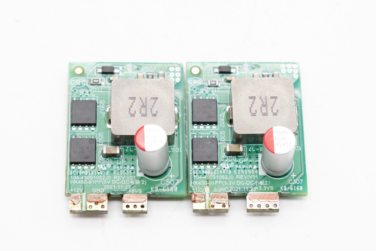
The 5V and 3.3V outputs are converted by independent PCBs. The output voltage is marked on the PCB, while the front features the buck inductor, buck switching MOSFETs, and filter caps.
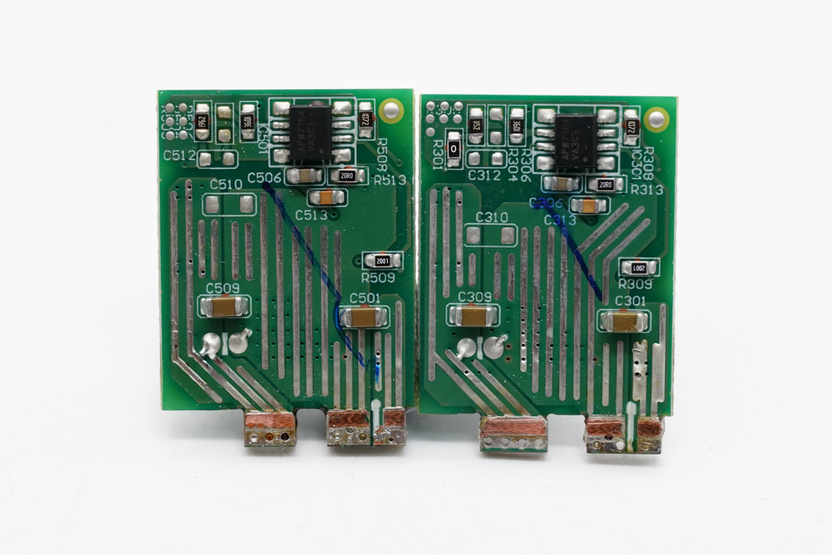
The back sides feature filter caps and a synchronous buck controller. The component configuration on both sides of the PCBs is identical.
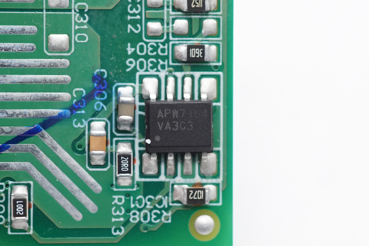
The synchronous buck controller is from ANPEC, model APW7164. It is a voltage-mode synchronous buck controller with integrated soft-start and a fixed switching frequency of 200kHz. It supports UVP and OVP and is housed in an SOP-8 package.
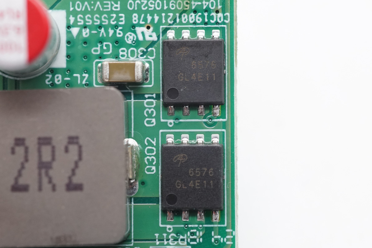
The synchronous buck switching MOSFET is from AOS, model AON6576, NMOS, 30V and 3.9mΩ. It features low gate charge and high current capability and is designed for DC/DC converter applications in computing and servers, as well as isolated DC/DC conversion in telecommunications and industrial applications. It is housed in a DFN5×6 package.
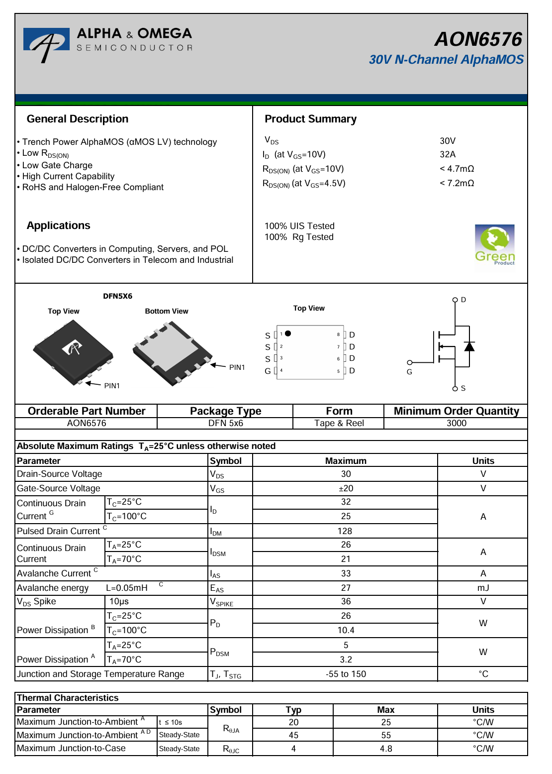
Here is the info about the AOS AON6576.
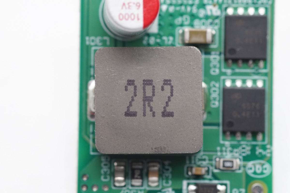
The 2.2μH buck inductor.
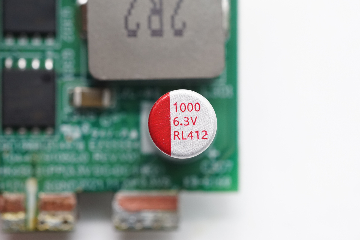
The filter cap is from PolyCap, part of the RL series, and rated at 1000μF 6.3V.
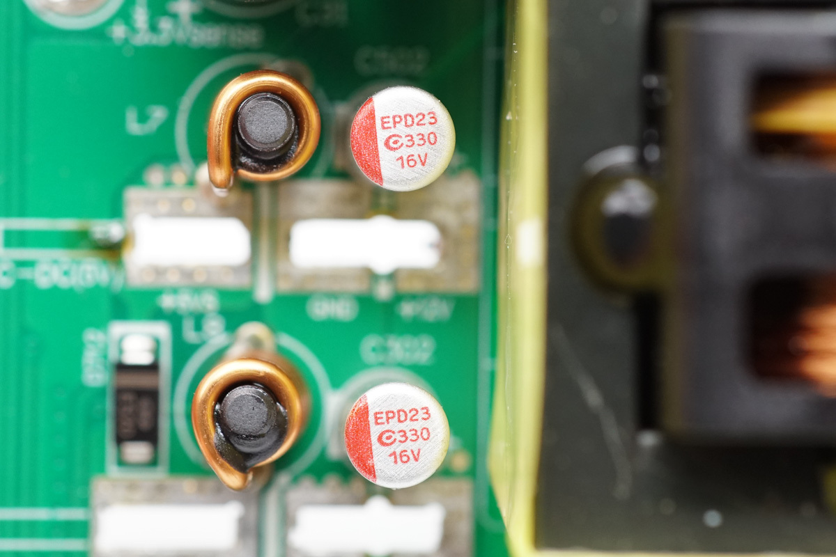
The filter caps are from APAQ and rated at 330μF 16V.
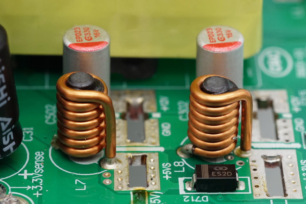
Filter inductors are installed at the output end of the buck PCB.
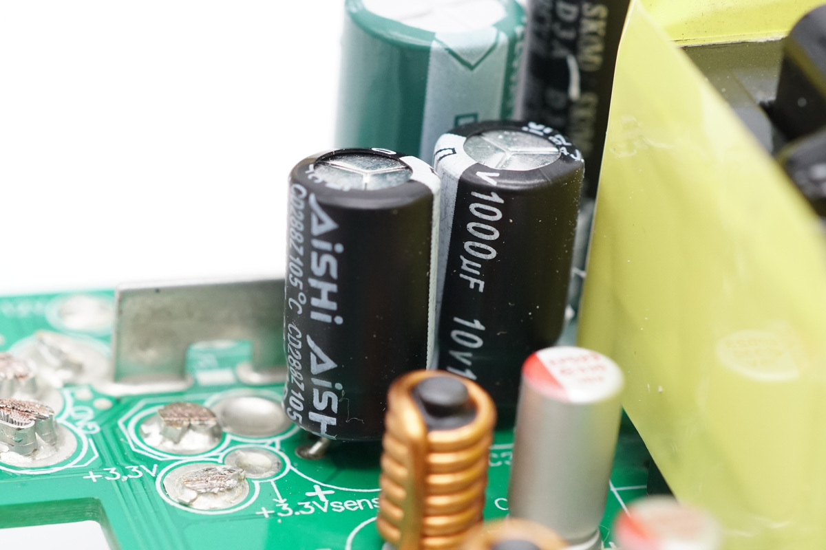
The filter caps are from AiShi and rated at 1000μF 10V.
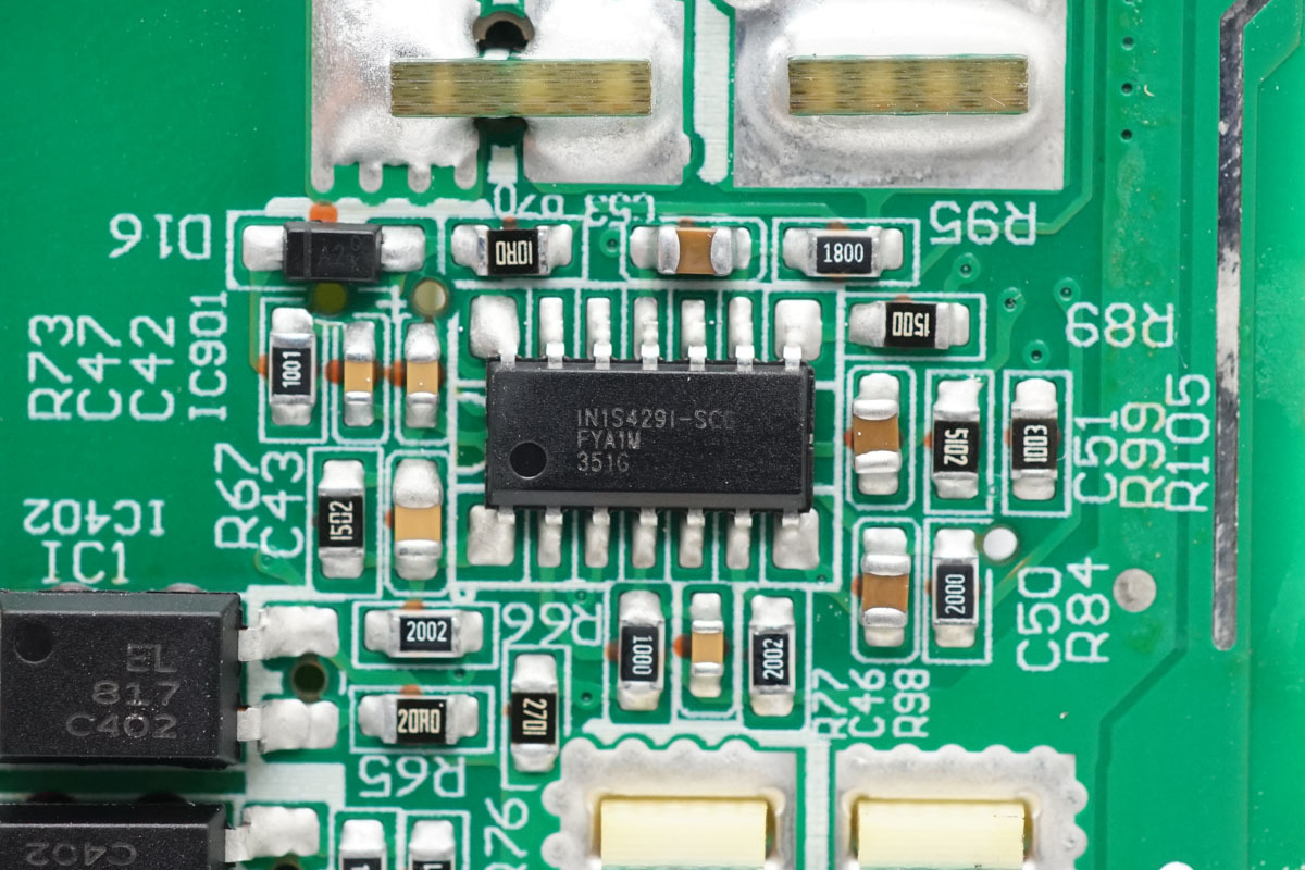
The power management IC is from infsitronix, model IN1S429I-SCG. It provides OVP, UVP, OCP, SCP, and OTP for the 3.3V, 5V, and 12V outputs. It is housed in an SOP-14 package.
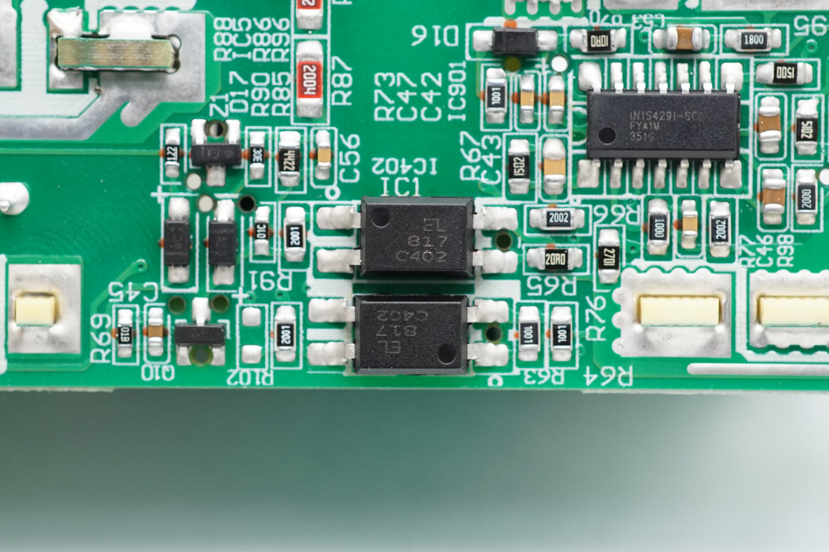
Two EL817 optocouplers are used for feedback isolation.
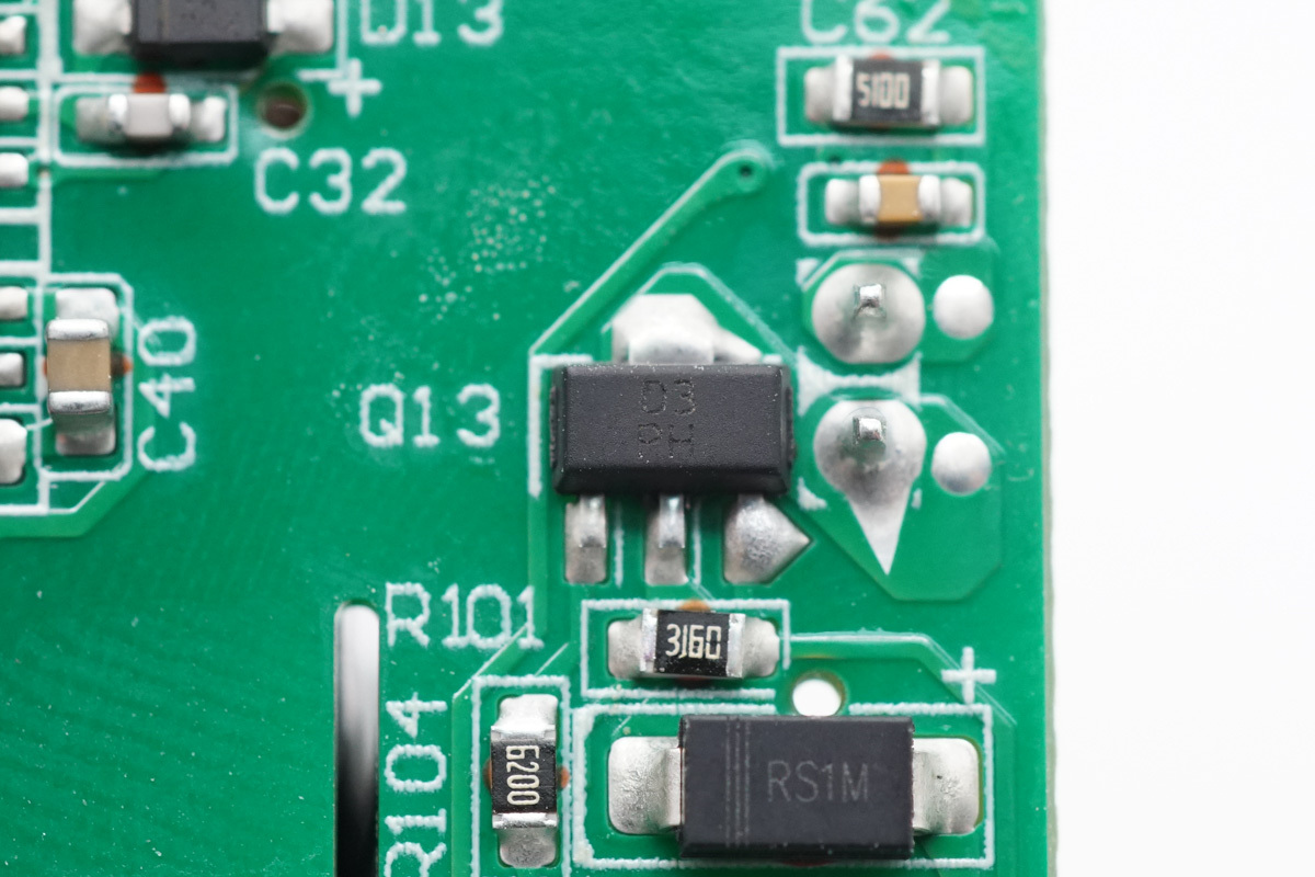
The transistor used to control the cooling fan.
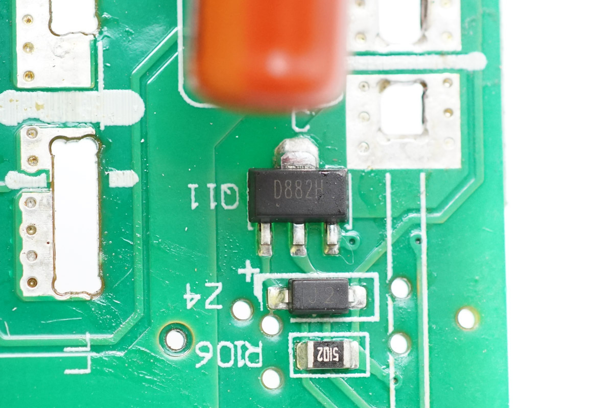
The transistor, marked D882H.
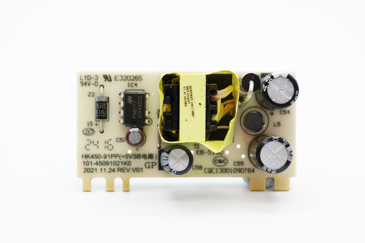
The standby power supply uses an independent PCB. The front side features the standby power supply controller, transformer, filter cap, and rectifier MOSFET.
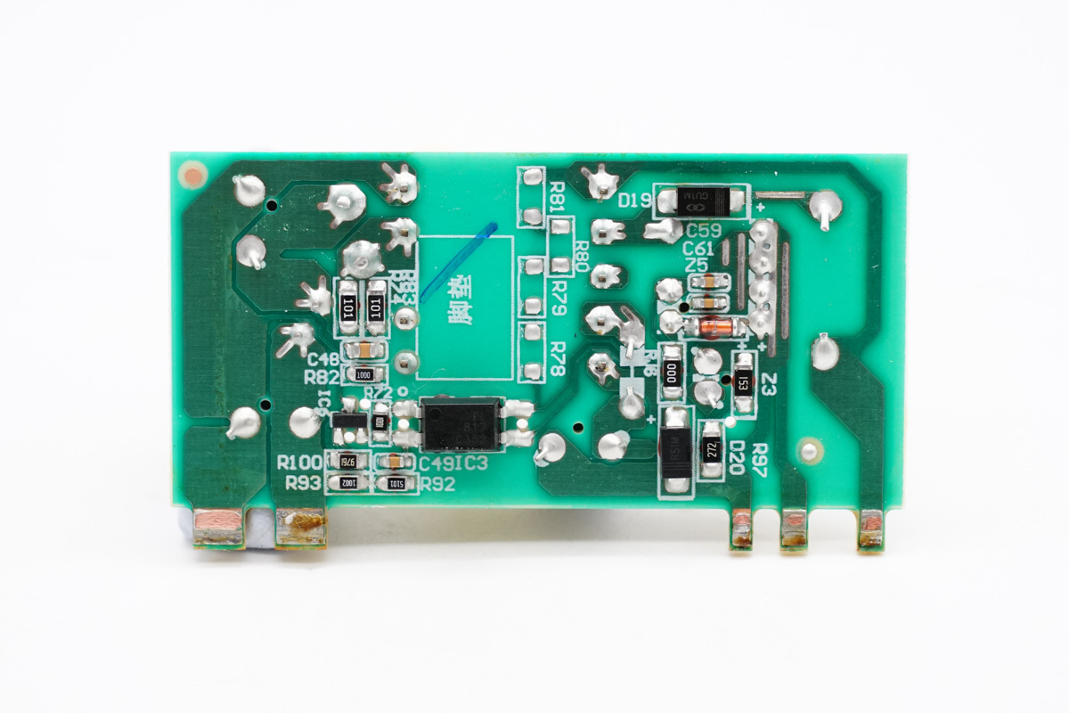
The back of the PCB features the feedback optocoupler.
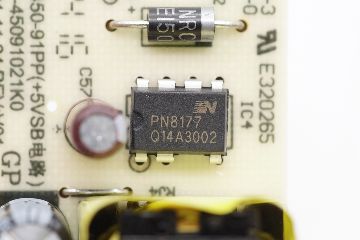
The standby power supply controller is from Chipown, model PN8177. It integrates a PFM controller and an 800V MOSFET, along with high-voltage startup and self-powered circuits, and provides comprehensive protection functions. It is housed in a DIP-7 package.
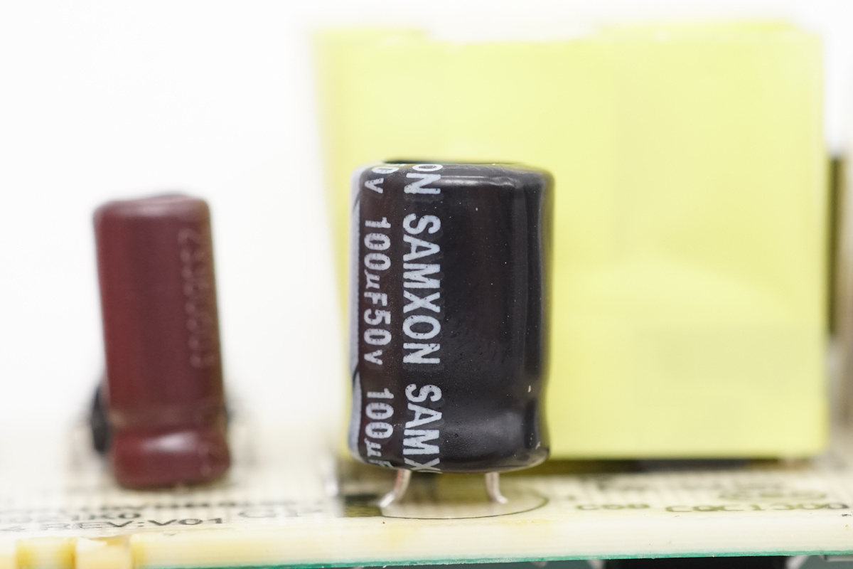
The power supply filter cap is from SAMXON and rated at 100μF 50V.
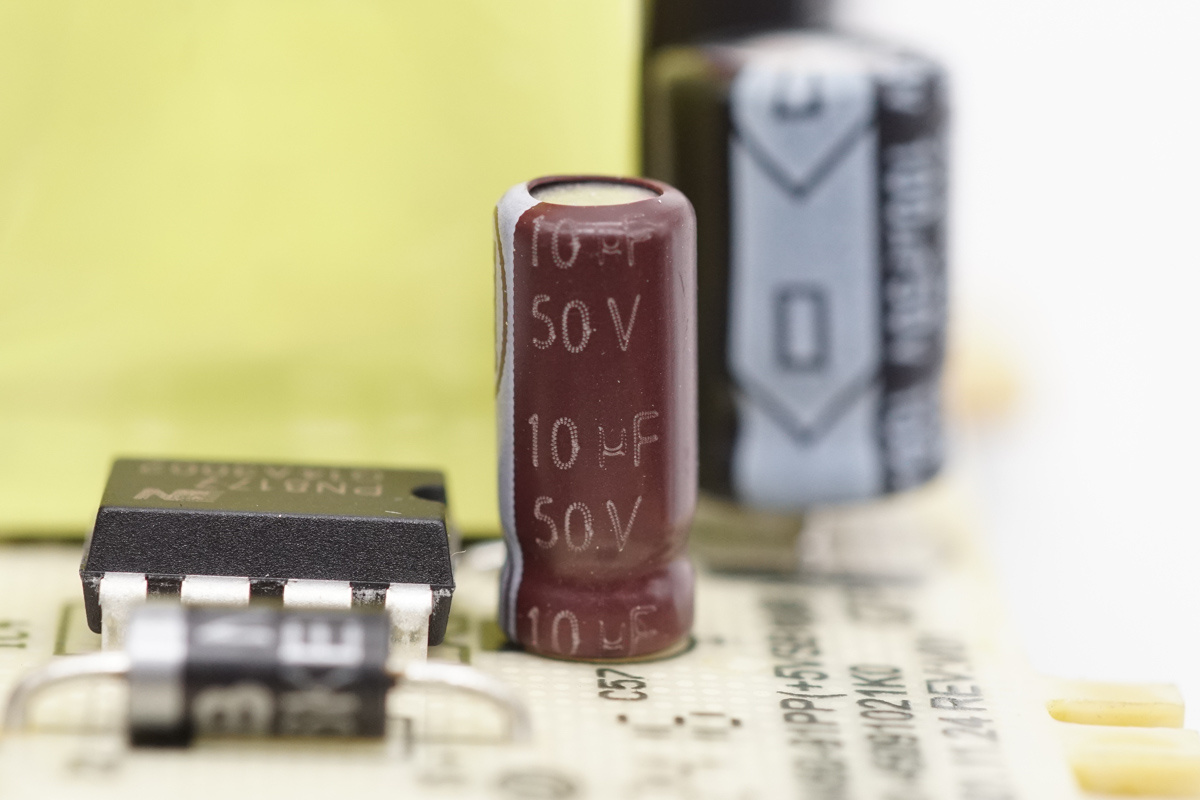
The other one is rated at 10μF 50V.
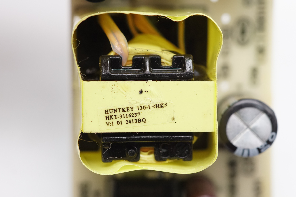
The transformer is tightly wrapped with insulating tape.
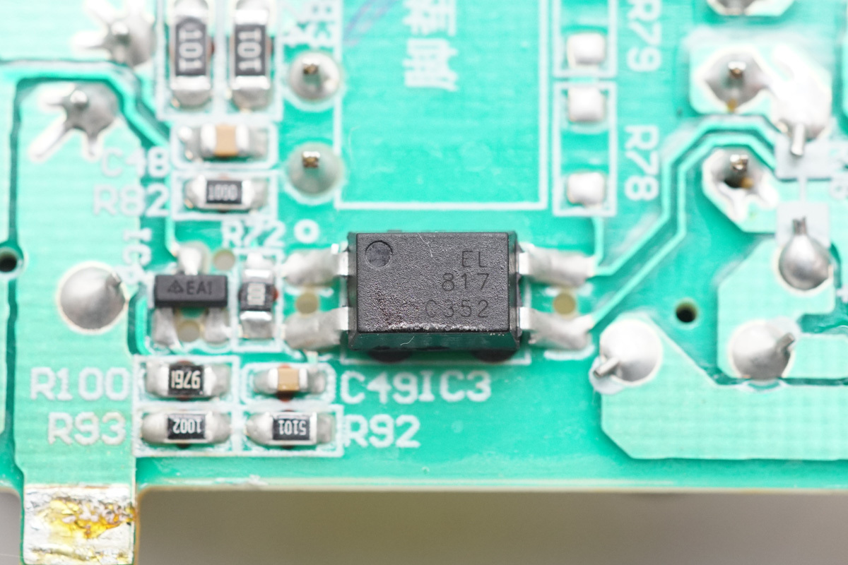
An EL817 optocoupler is used for output voltage feedback.
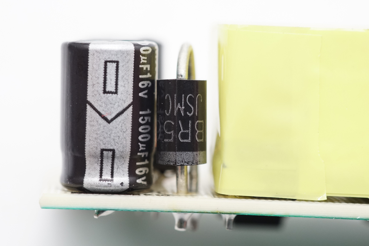
The rectifier MOSFET is from JSMC, model SBR560. It is a Schottky diode rated at 5A 60V and housed in a DO-201AD package.
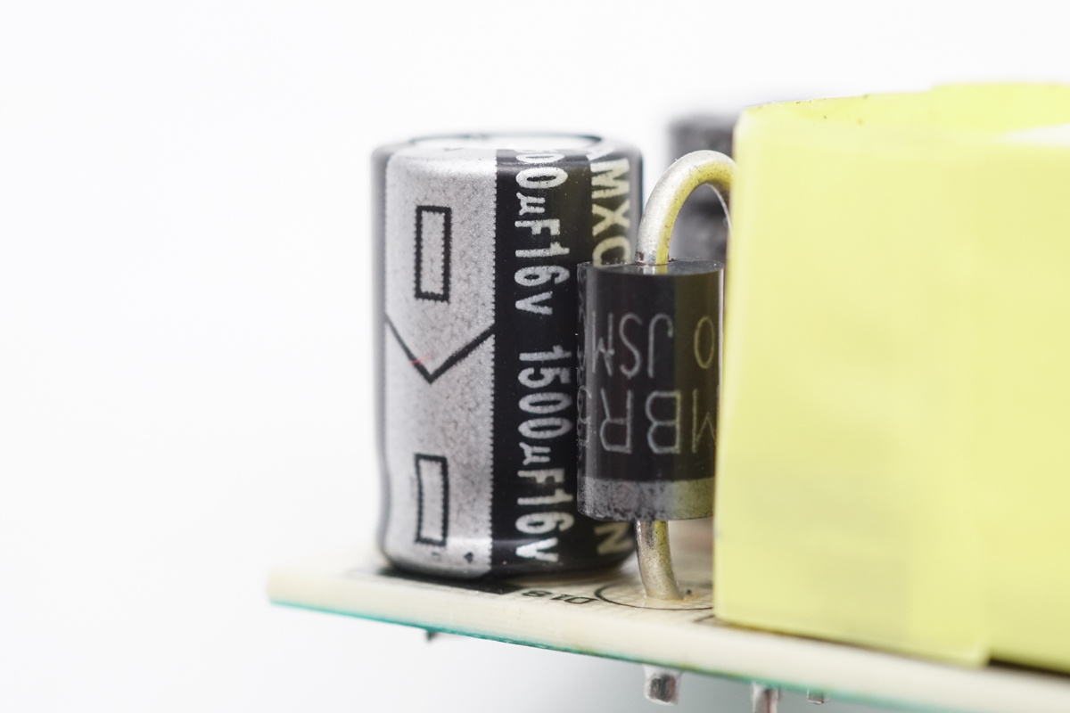
The filter cap is from SAMXON and rated at 1500μF 16V.
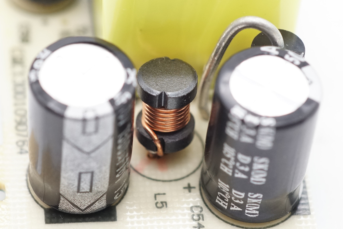
The filter inductor is wound with enameled wire.
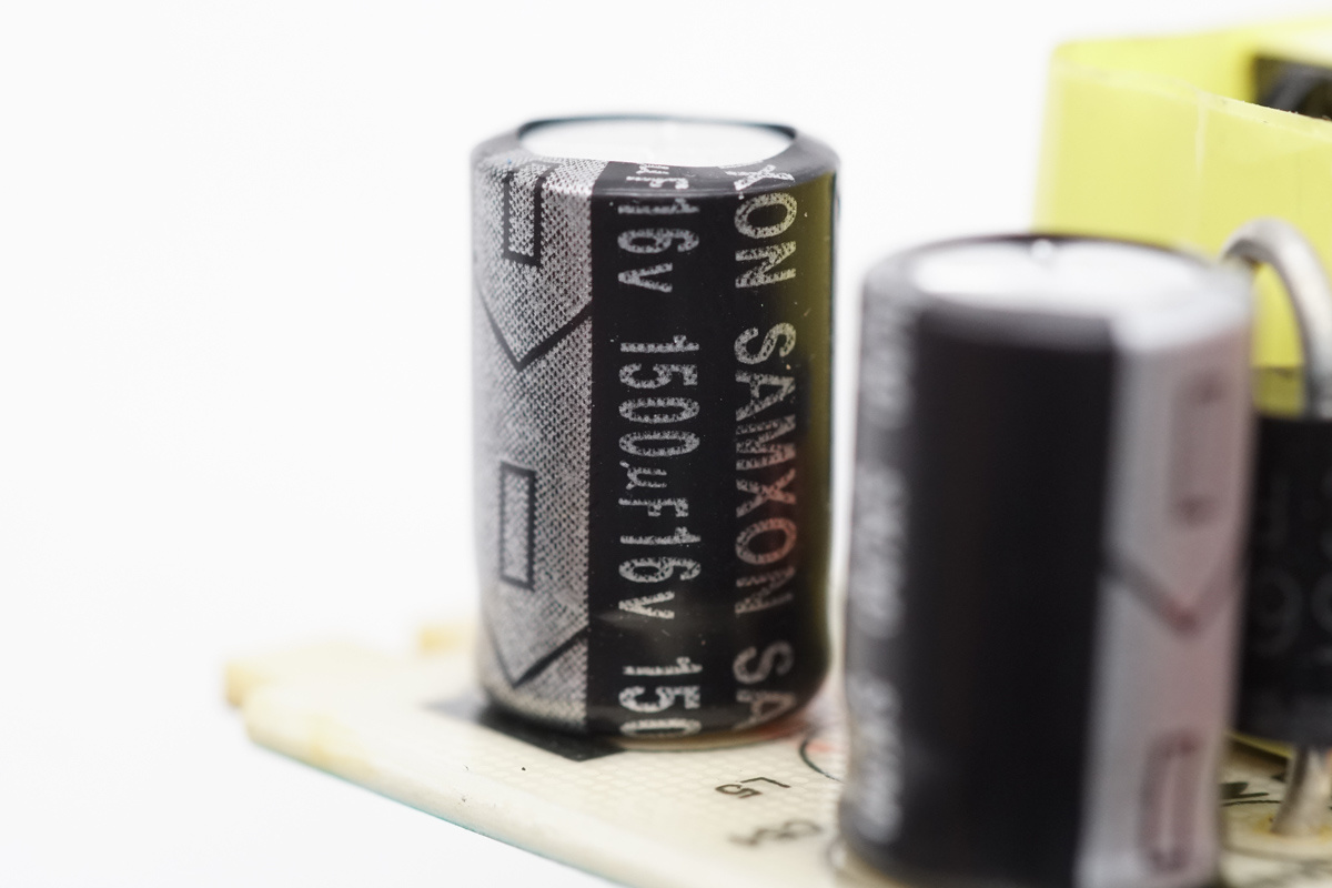
The other one shares the same spec.
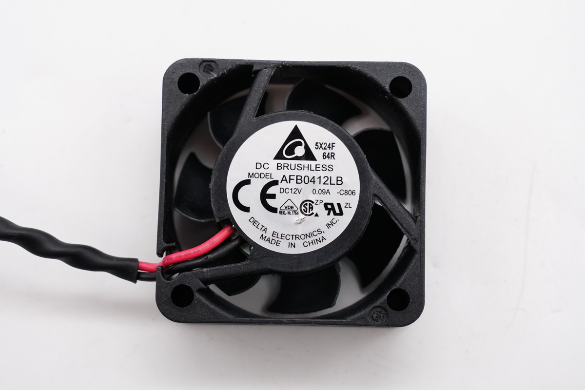
The cooling fan is from Delta, model AFB0412LB, rated at 12V 0.09A, made in China.
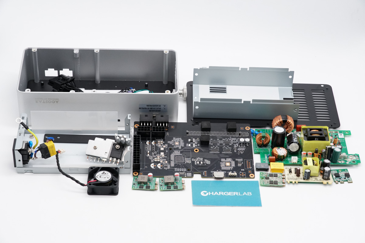
Well, those are all components of the AOOSTAR AG01 OCuLink eGPU Dock.
Summary of ChargerLAB
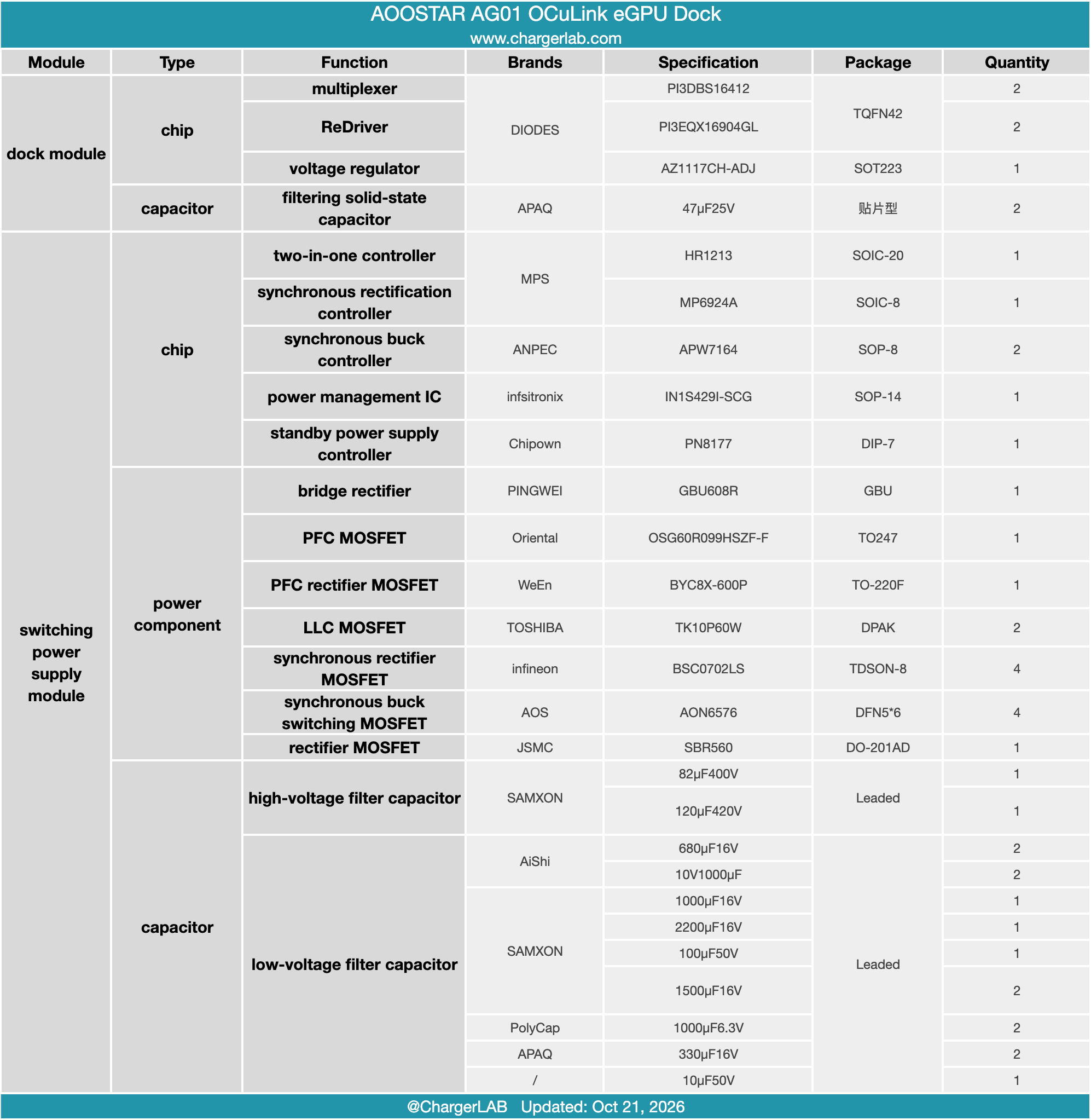
The AOOSTAR AG01 OCuLink eGPU Dock combines a sleek aluminum alloy chassis with an integrated internal power supply for a clean, premium look. Up front, an OCuLink port delivers high-speed PCIe 4.0×4 bandwidth to connected laptops or mini PCs. Dual 8-pin power headers feed the GPU via included power cables, while a top-facing PCIe slot paired with side mounting screws makes graphics card installation quick and rock-solid.
ChargerLAB's teardown shows the AG01 houses two distinct sub-assemblies: a dock module and a switching power supply module, linked via heavy-duty plug-in connectors. On the dock module , a DIODES PI3DBS16412 multiplexer handles signal switching, a PI3EQX16904GL ReDriver optimizes PCIe signal integrity across the cable, and an AZ1117CH linear regulator cleans up auxiliary power rails.
The switching power supply module comes from industry veteran Huntkey, built around an MPS HR1213 PFC+LLC combo controller and an MP6924A synchronous rectifier driver. Power MOSFET selection includes an Oriental OSG60R099HSZF-F for PFC switching, a WeEn BYC8X-600P PFC boost diode, TOSHIBA TK10P60W MOSFETs for the LLC stage, and Infineon BSC0702LS FETs for synchronous rectification.
Buck conversion for the 3.3V and 5V auxiliary rails is managed by an ANPEC APW7164 controller pairing AOS AON6576 power MOSFETs. Standby power is handled by a Chipown PN8177 primary IC, backed by a high-grade cap bank featuring SAMXON, AiShi, PolyCap, and APAQ units. Inside and out, the AG01 demonstrates name-brand component selection and solid engineering quality.
Related Articles:
1. Review of AOOSTAR GEM12 Pro Mini PC
2. AOOSTAR, MINISFORUM, METAPHYUNI and Others Launch a Variety of Mini PCs that Support OCuLink
3. OCuLink | Review of AOOSTAR AG01 OCuLink GPU Dock