

Introduction
In this teardown, we are taking a deep dive into the Apple Mac Studio. At its heart sits the M5 Max chip—built on TSMC’s advanced N3P process node—packing an 18-core CPU (6 Super cores + 12 Performance cores) and a 32-core GPU. Unified memory spans from 36GB to 256GB alongside 512GB to 8TB storage, while the top-tier M5 Ultra variant scales up to 512GB memory and 16TB storage.
On the I/O front, the Mac Studio features dual USB-C ports, an SD card reader, and a power LED up front. Flipping to the back reveals four high-speed Thunderbolt 5 ports, two USB-A ports, 10Gb Ethernet, and an HDMI port. Next, let’s join ChargerLAB as we strip down the Apple Mac Studio to inspect its internal engineering and component selection.
Product Appearance
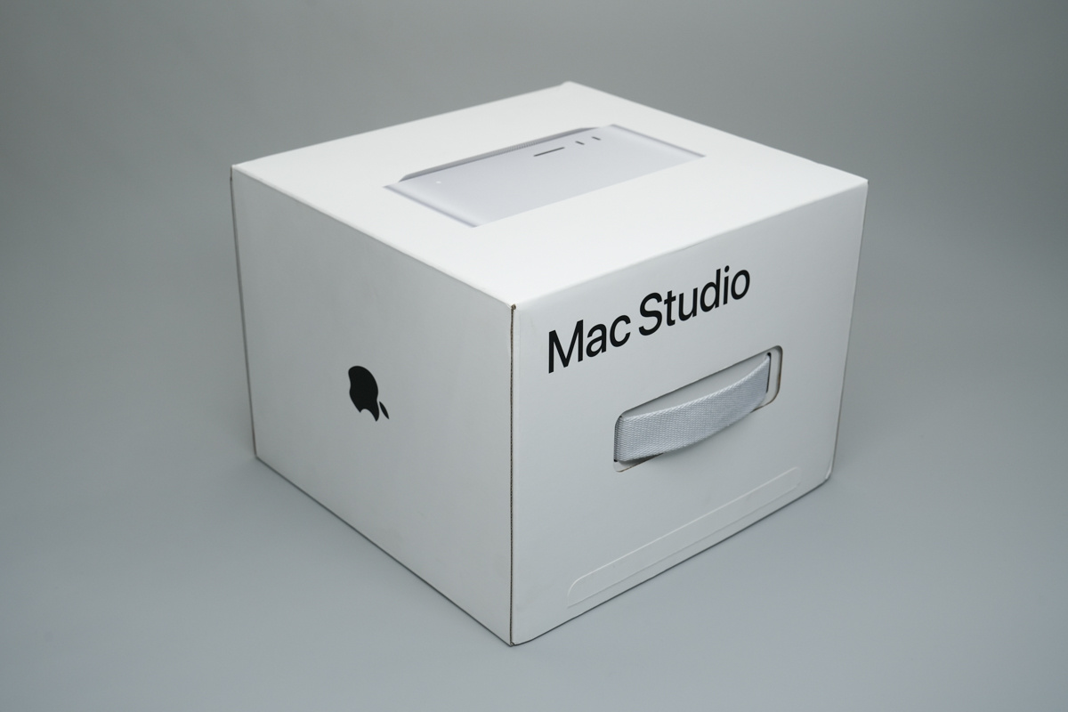
The Apple Mac Studio comes in a cube-shaped box featuring images of the computer's front panel, the Apple logo, and the "Mac Studio" branding on three sides.
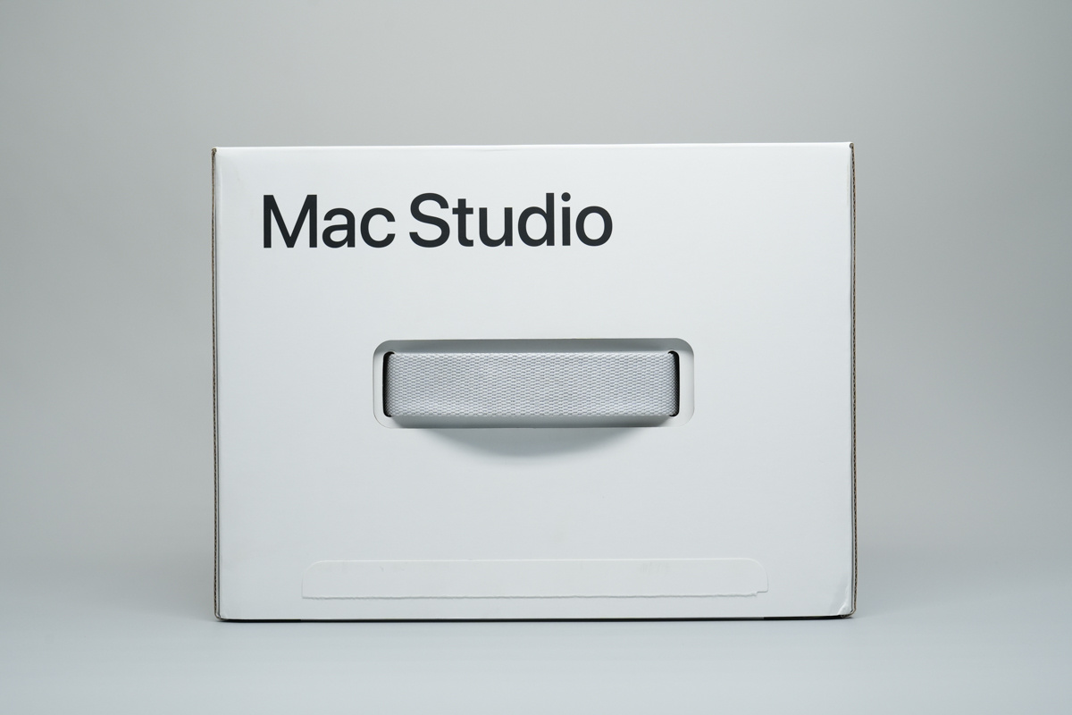
A carrying handle is provided on the top of the box.
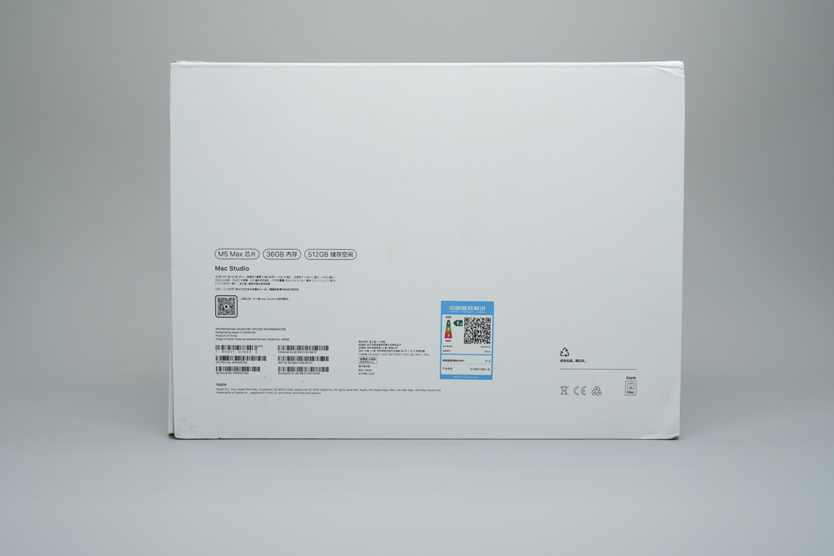
Product info is printed on the side of the box.
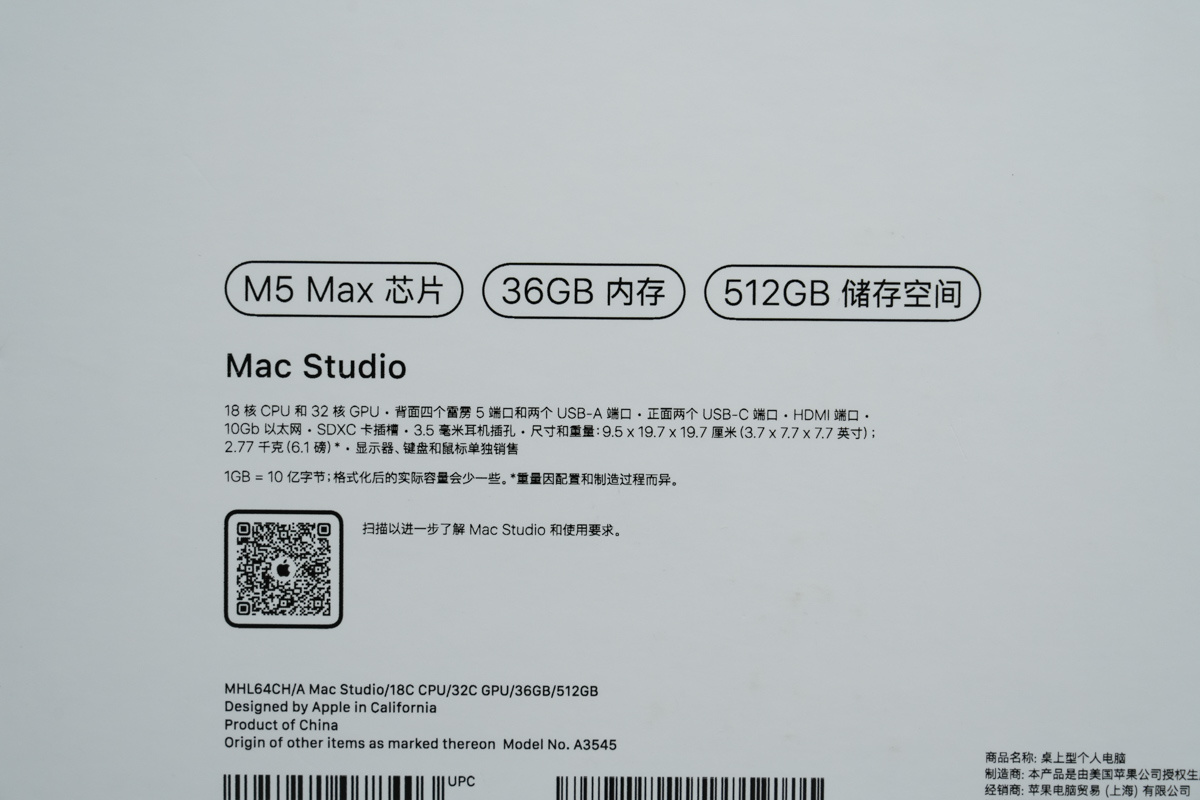
The Apple Mac Studio is equipped with the M5 Max chip, 36GB of memory, and 512GB of storage. The M5 Max features an 18-core CPU and a 32-core GPU. The computer features four Thunderbolt 5 ports, two USB-A ports, two USB-C ports, an HDMI port, a 10Gb Ethernet port, and an SDXC card slot. The model number is MHL64CH/A, and the device model is A3545.
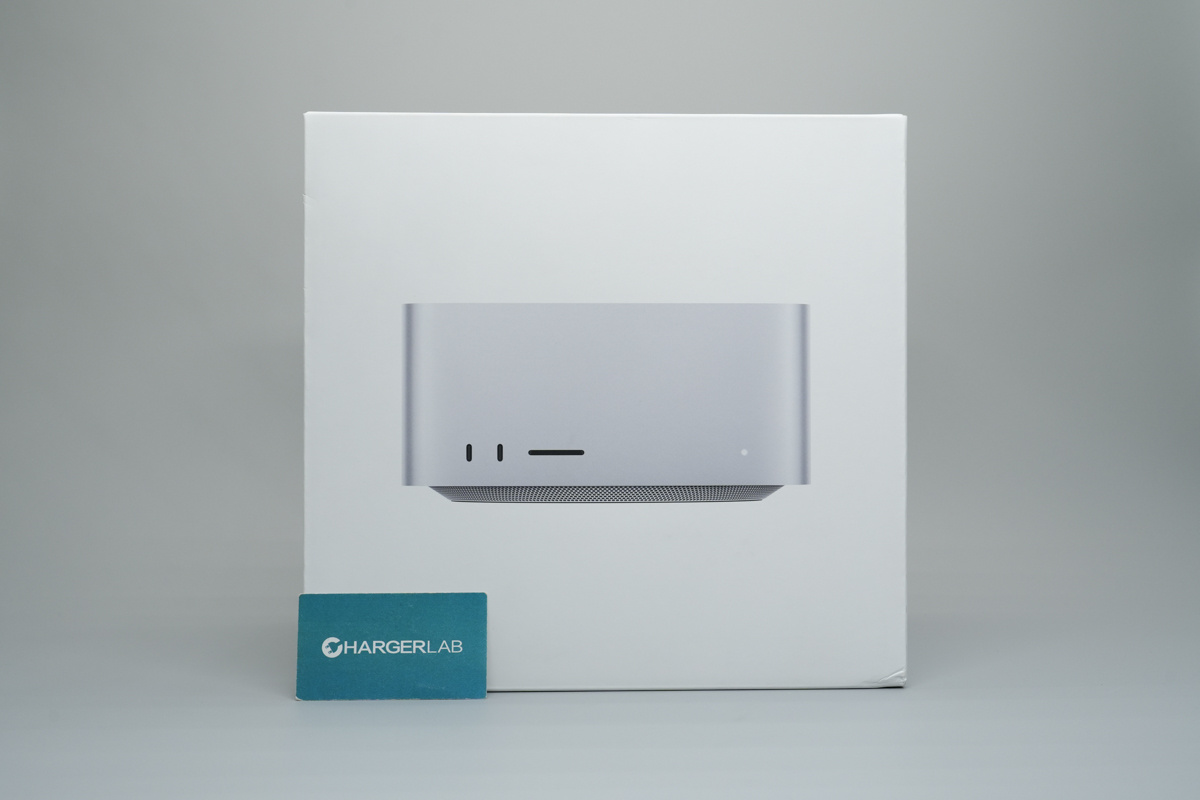
The front of the Mac Studio is pictured on the front of the box.
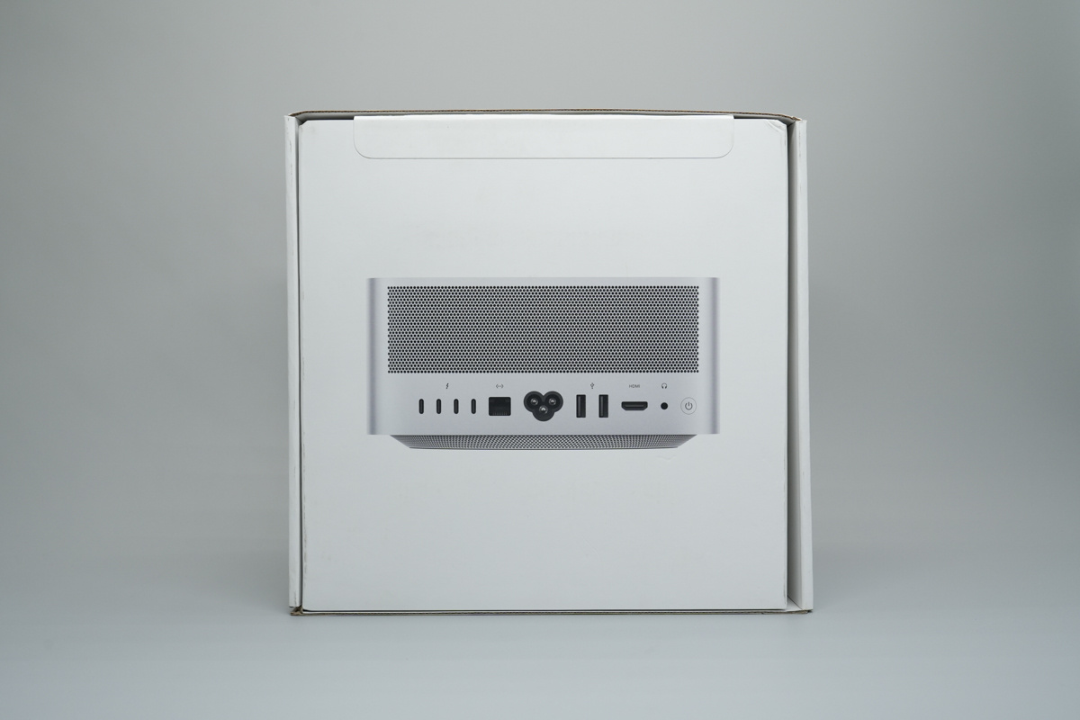
The rear of the computer is pictured on the back of the box.
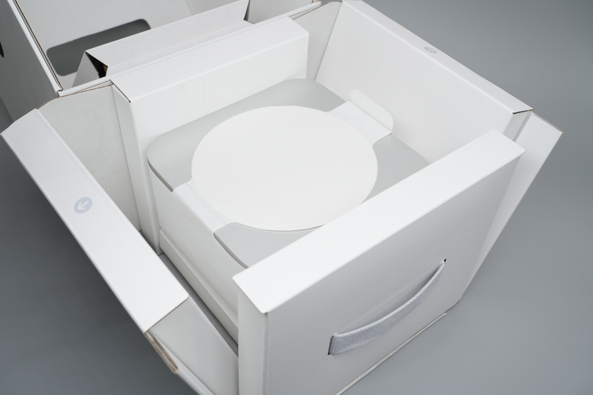
After removing the seal, the box opens to reveal the computer secured in a cardboard insert.
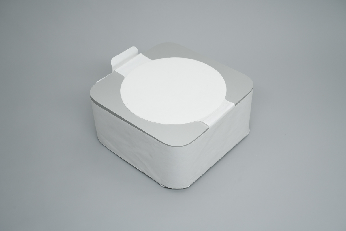
A protective film is applied to the surface of the computer.
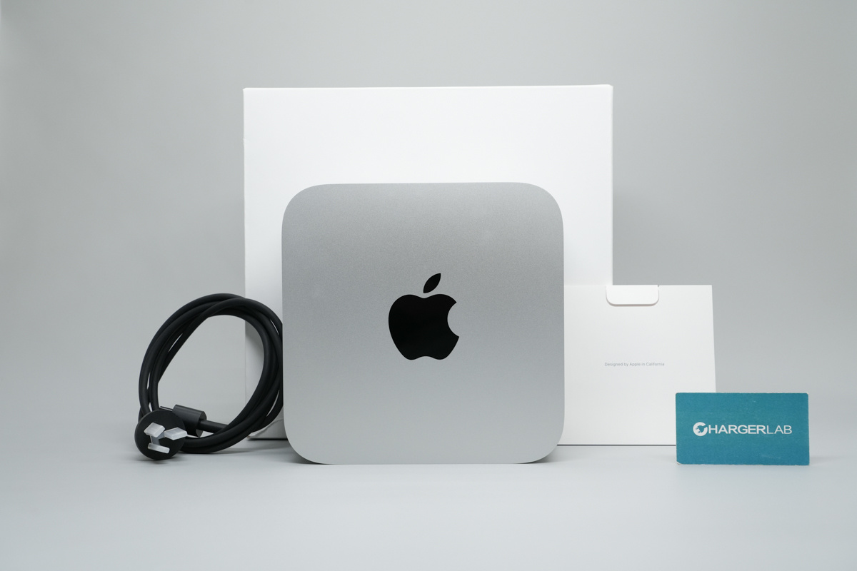
The package contains the Apple Mac Studio, a power cord, a user manual, and a warranty card.
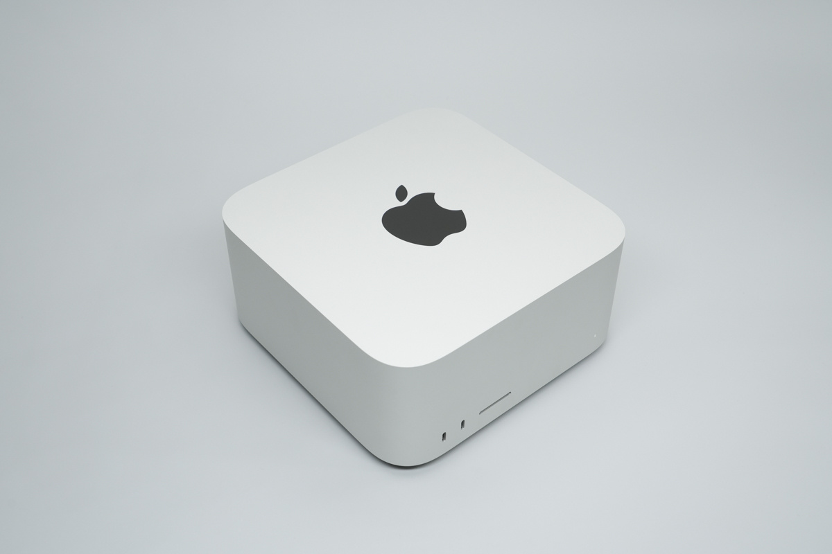
An Apple logo is located on the top of the computer.
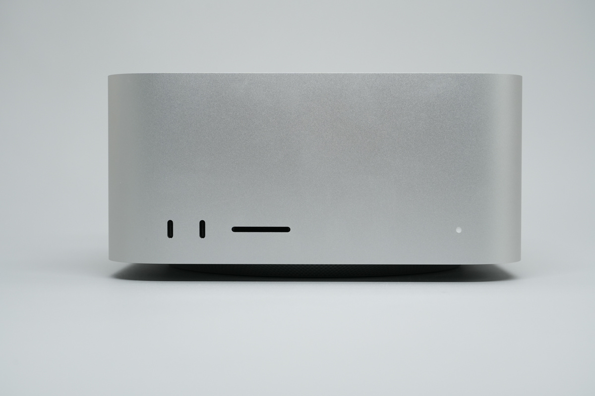
The front panel features two USB-C ports, an SD card slot, and a power indicator.
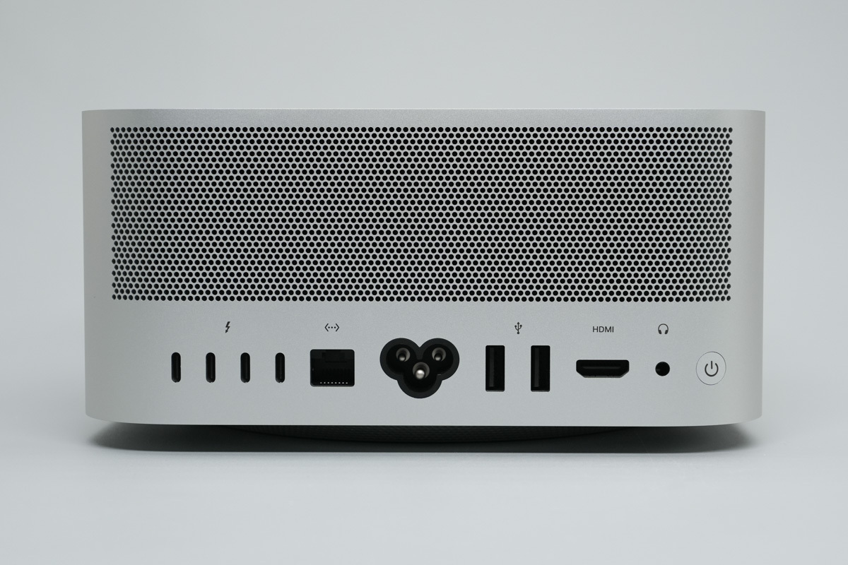
The rear panel features a large ventilation area at the top. The lower section houses the Thunderbolt 5 ports, Ethernet port, AC power inlet, USB-A ports, HDMI port, 3.5mm audio jack, and power button.
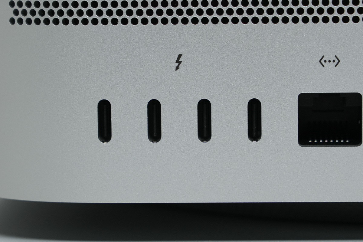
The four Thunderbolt 5 ports on the rear panel.
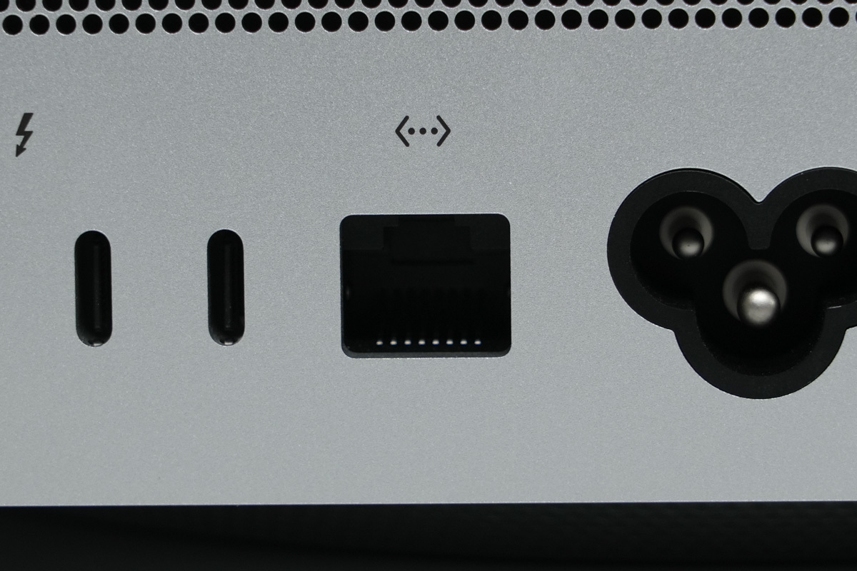
The 10Gb Ethernet port.
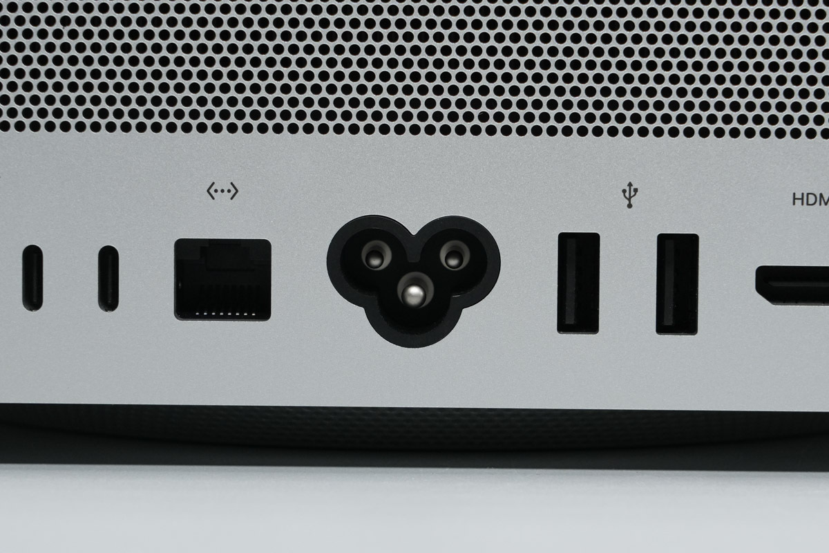
The cloverleaf AC power inlet.
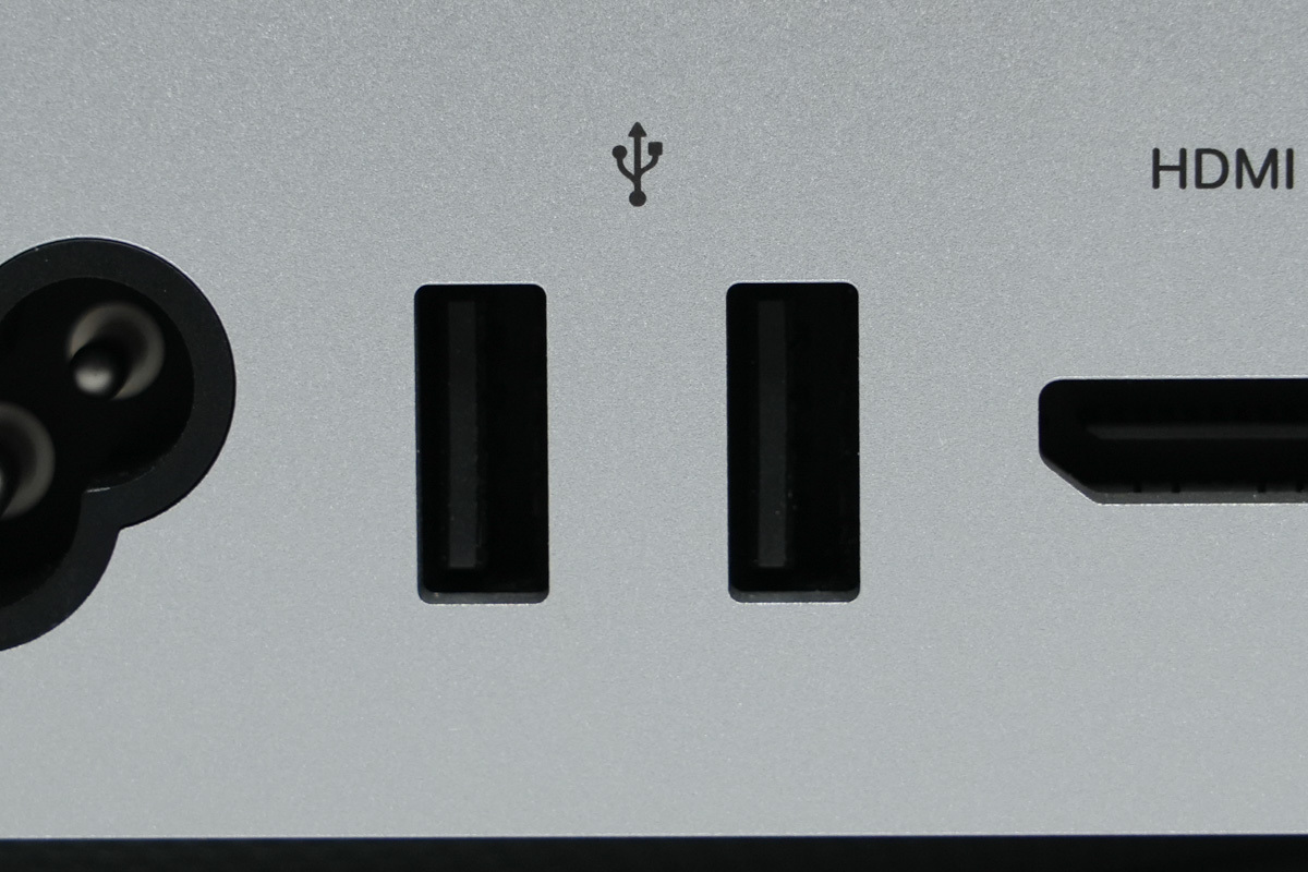
The USB-A ports.
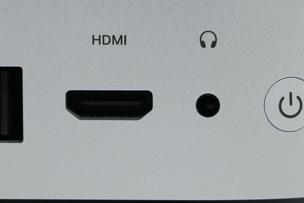
The HDMI port and 3.5mm audio jack.
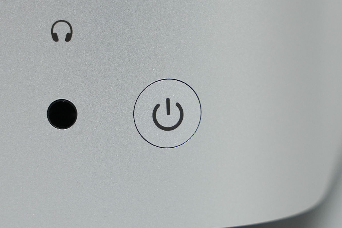
The power button.
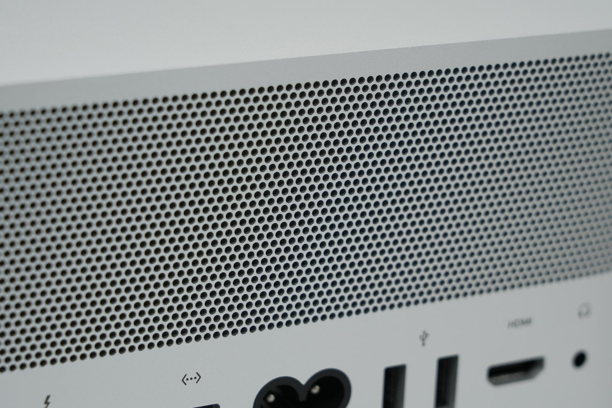
The rear ventilation area.
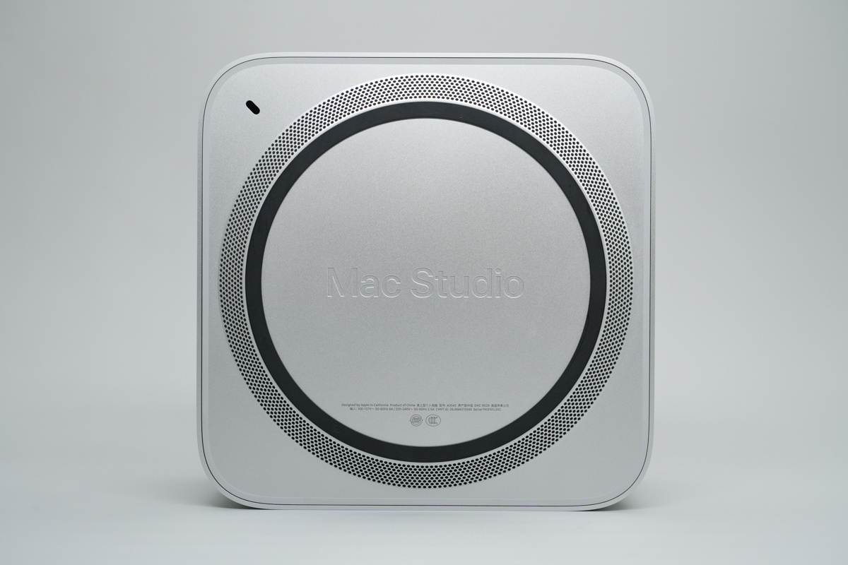
The bottom of the computer features an aluminum alloy cover with a circular anti-slip ring, ventilation openings, and a security lock slot.
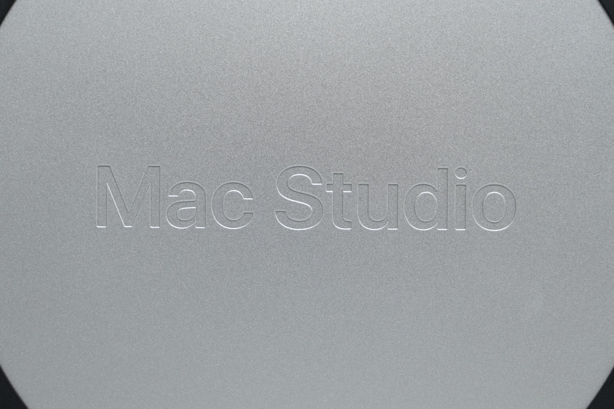
The "Mac Studio" wordmark is printed on the bottom of the computer.
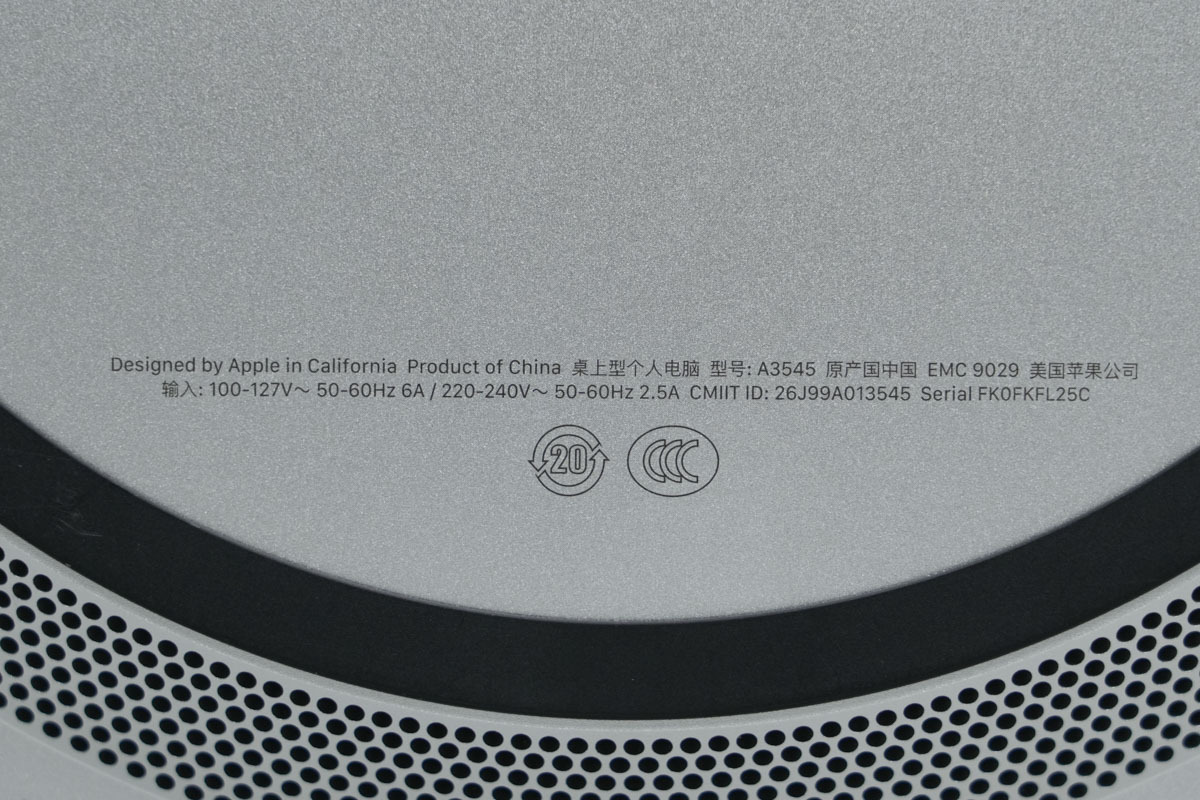
The bottom label identifies the product as a desktop computer, model A3545, manufactured in China by Apple Inc., USA. The input specifications are 100–127V~ 50–60Hz 6A / 220–240V~ 50–60Hz 2.5A. The product has obtained CCC certification.
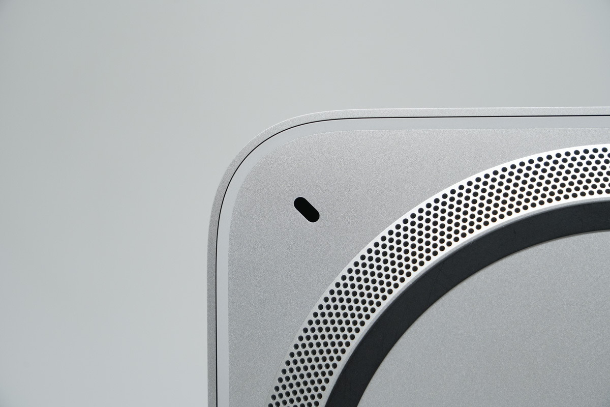
The security lock slot on the bottom.
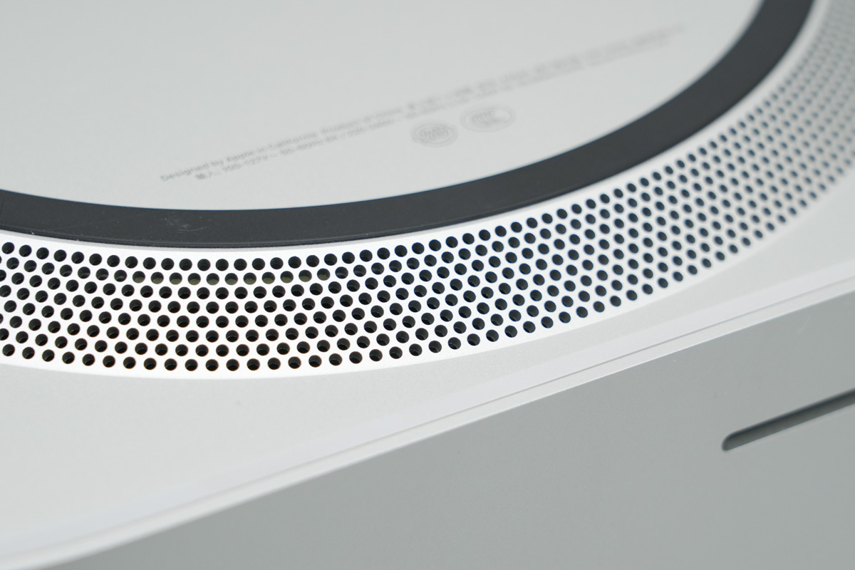
The ventilation openings on the bottom.
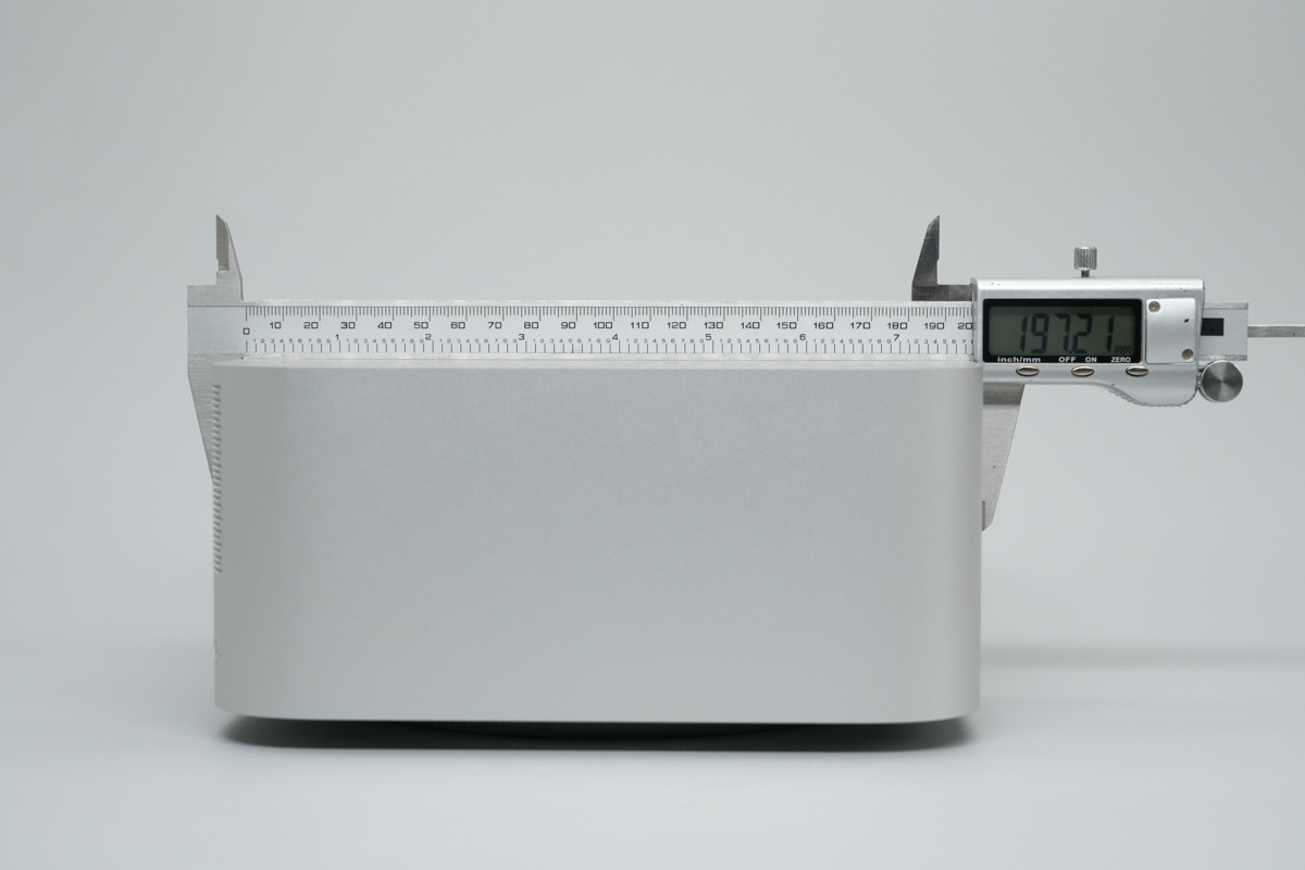
The length of the Mac Studio is about 197.2mm (7.764 inches).
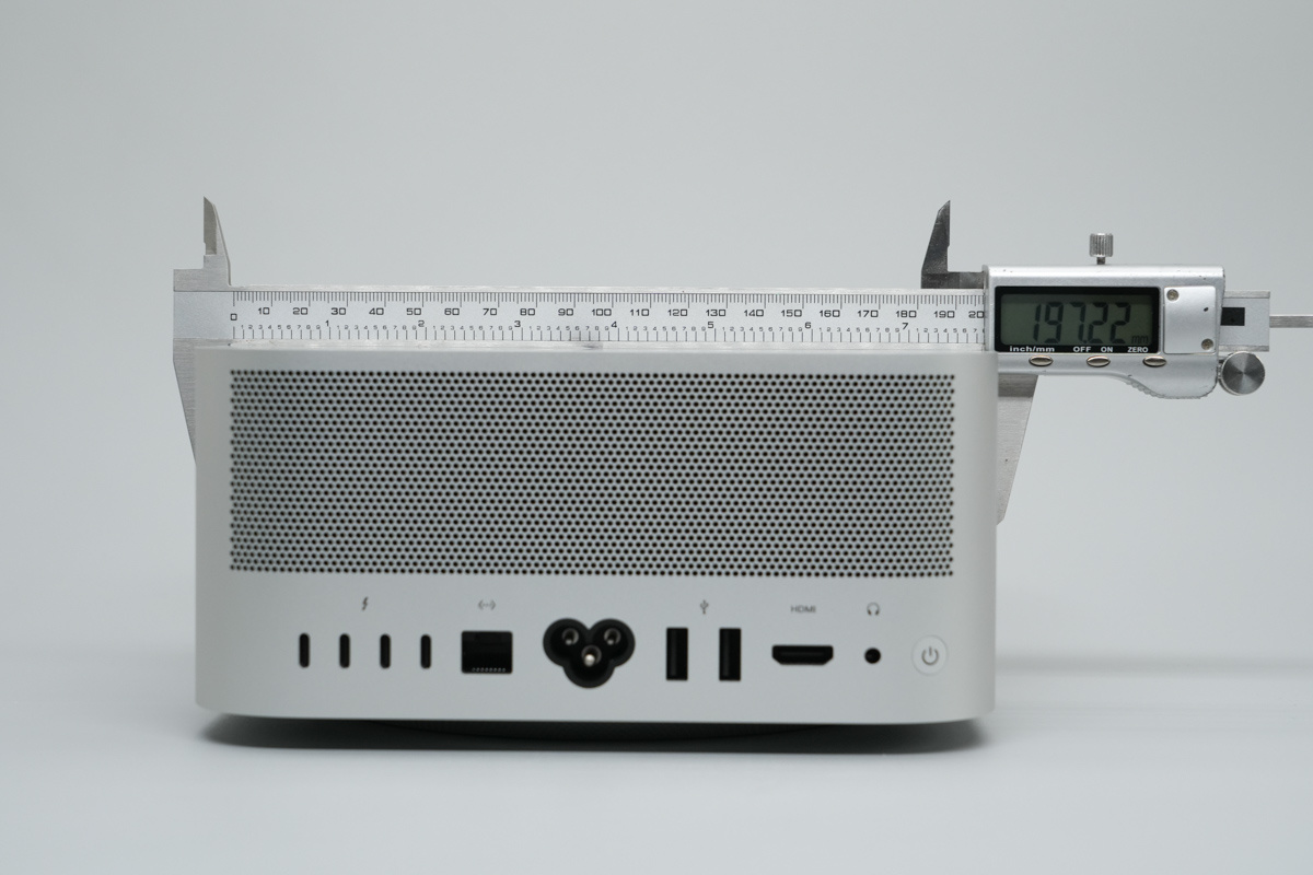
The width of the Mac Studio is about 197.2mm (7.764 inches).
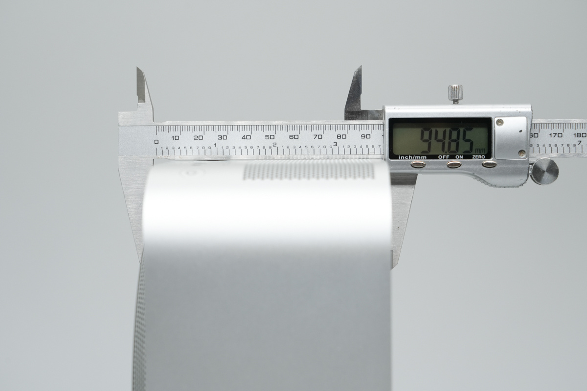
The thickness of the Mac Studio is about 94.9mm (3.736 inches).
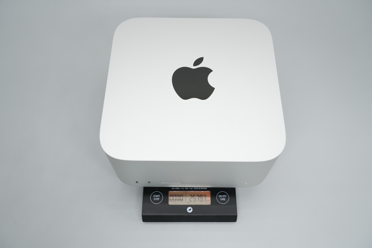
The weight is about 2580g (91.007 oz).
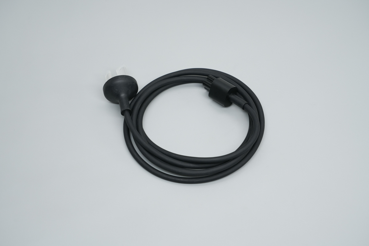
The included power cord features a three-prong plug.
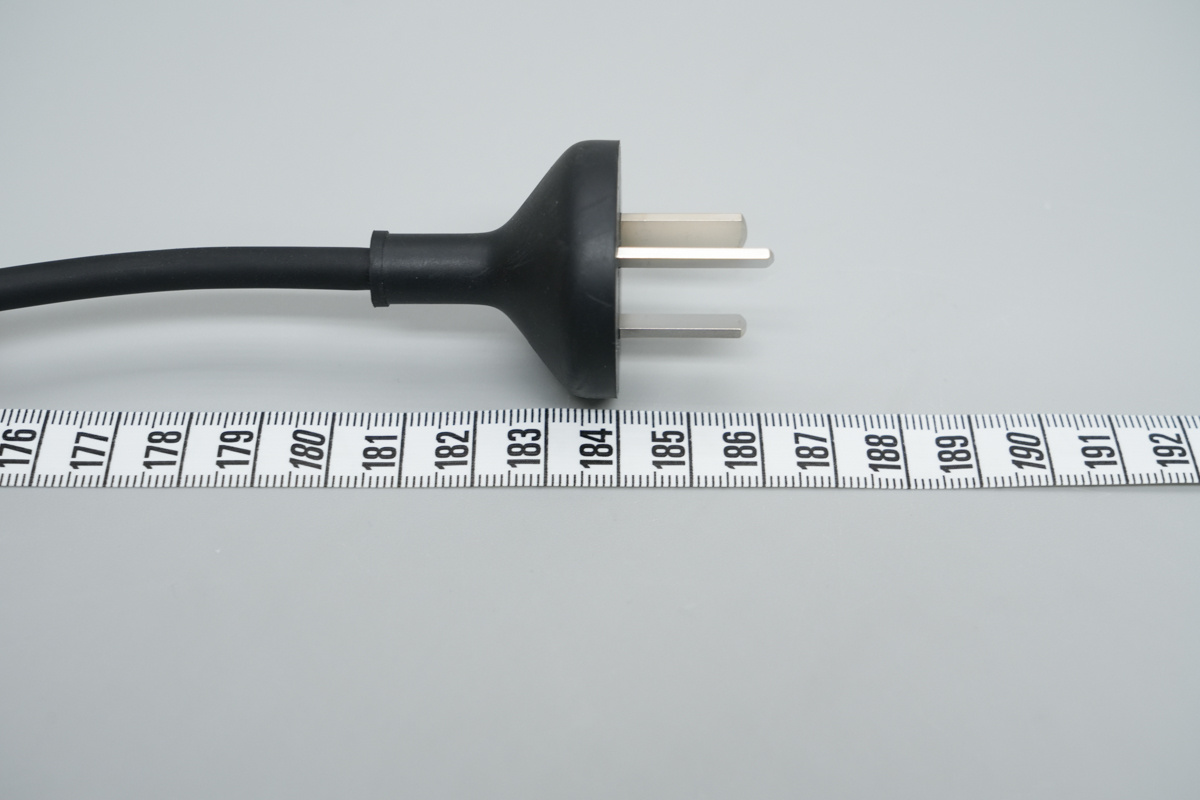
The length of the power cord is about 186cm (73.228 inches).
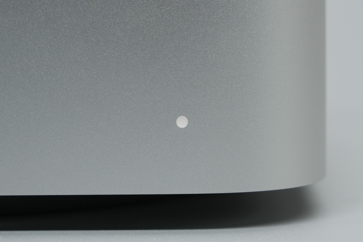
Once connected to power and switched on, the Mac Studio's power indicator lights up.
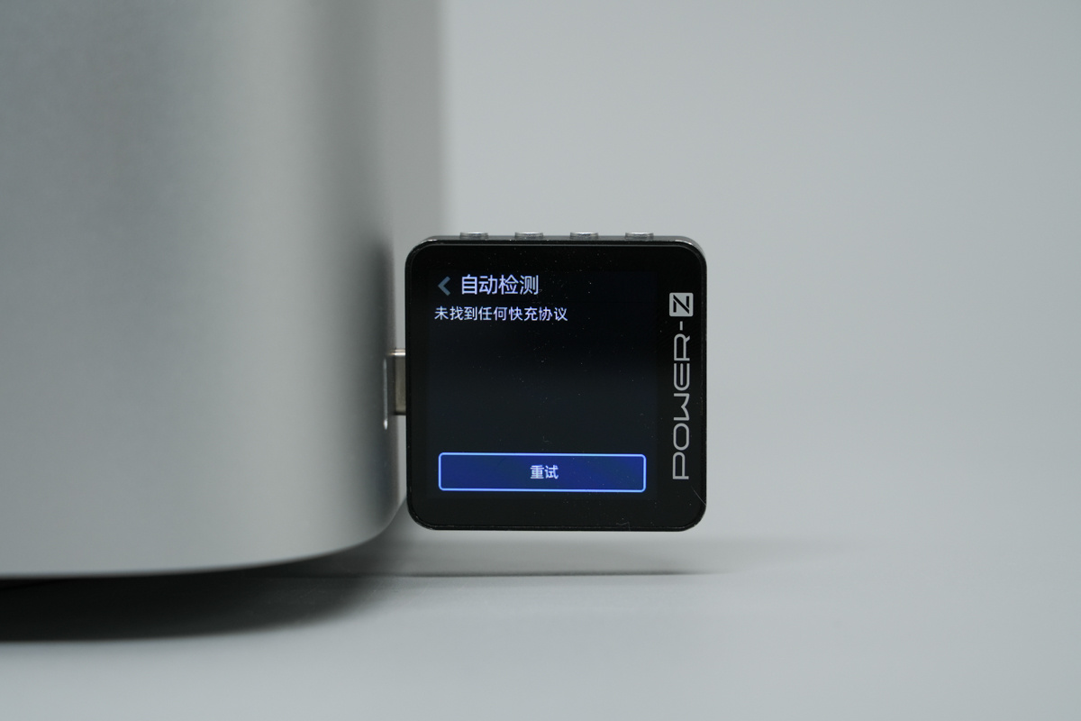
ChargerLAB POWER-Z KM003C shows that the two front USB-C ports do not support any fast-charging protocols.
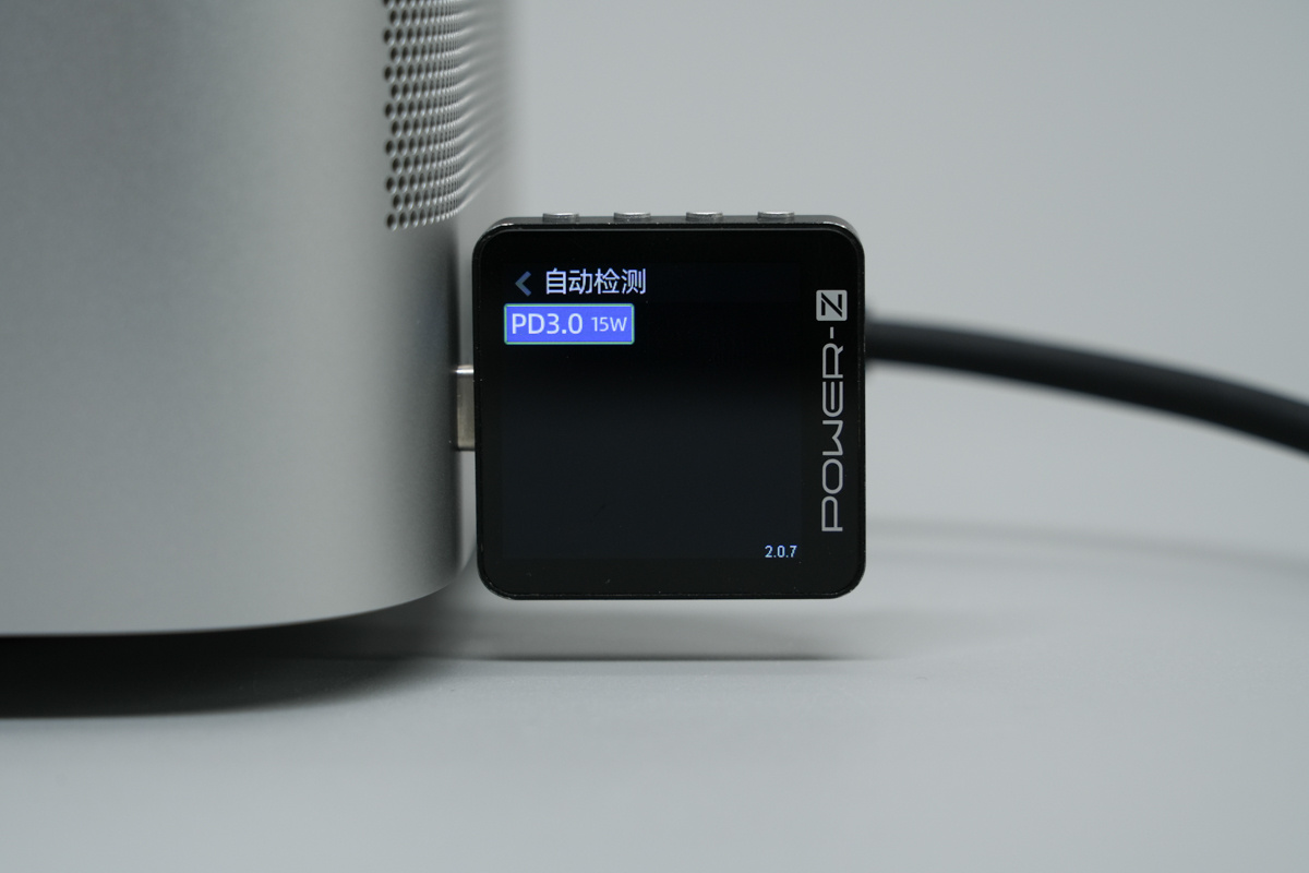
All four rear USB-C ports support the PD 3.0 protocol.
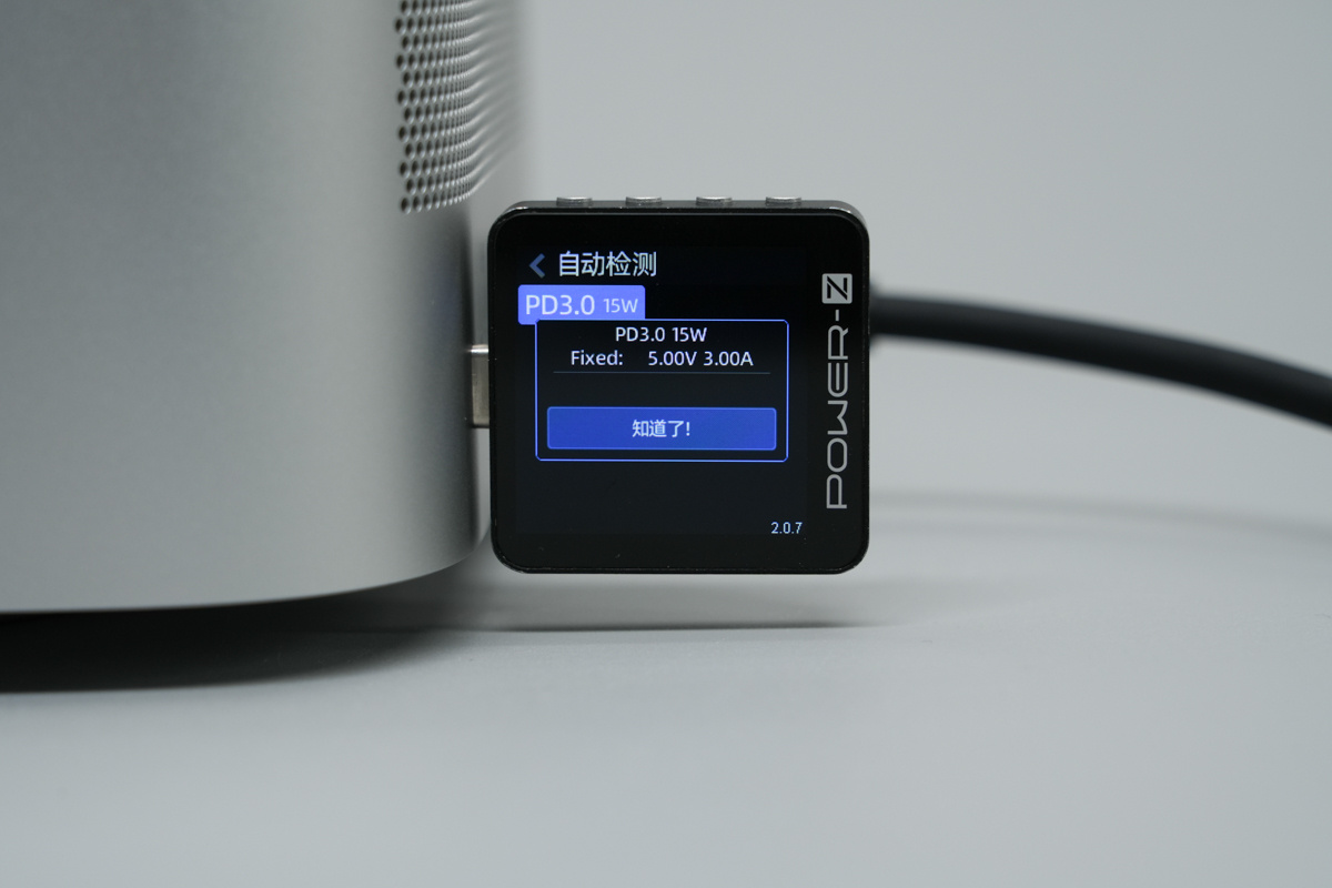
The PDO report shows that each USB-C port supports a fixed 5V 3A output profile. All four ports offer the same PDO profile.
Teardown
After the unboxing, let's take apart the Apple Mac Studio and examine its internal design and components.
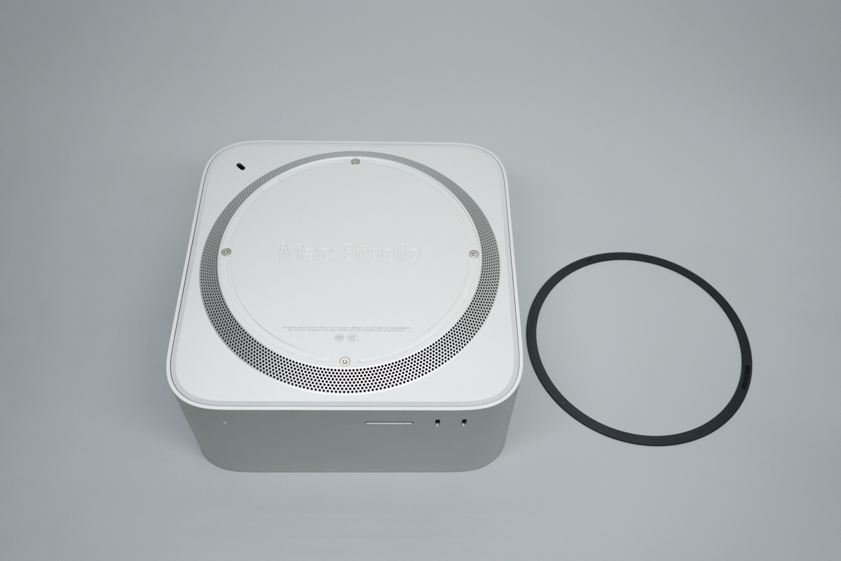
First, remove the anti-slip ring from the bottom.
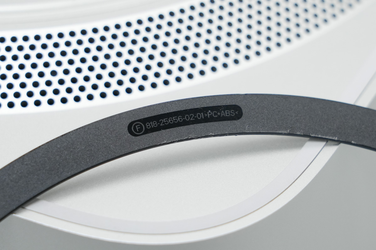
The anti-slip ring is made of PC+ABS material.
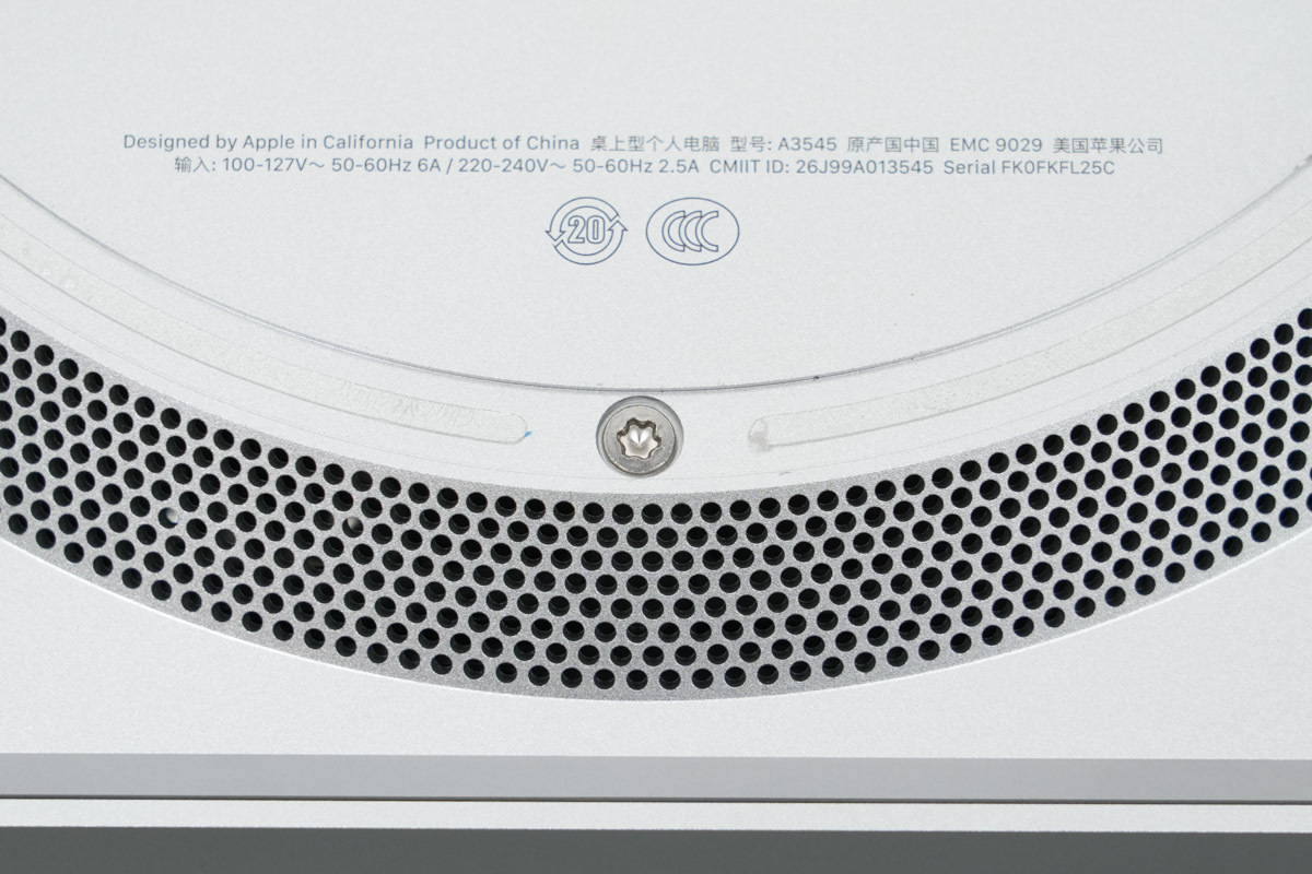
Mounting screws are located underneath the anti-slip ring.
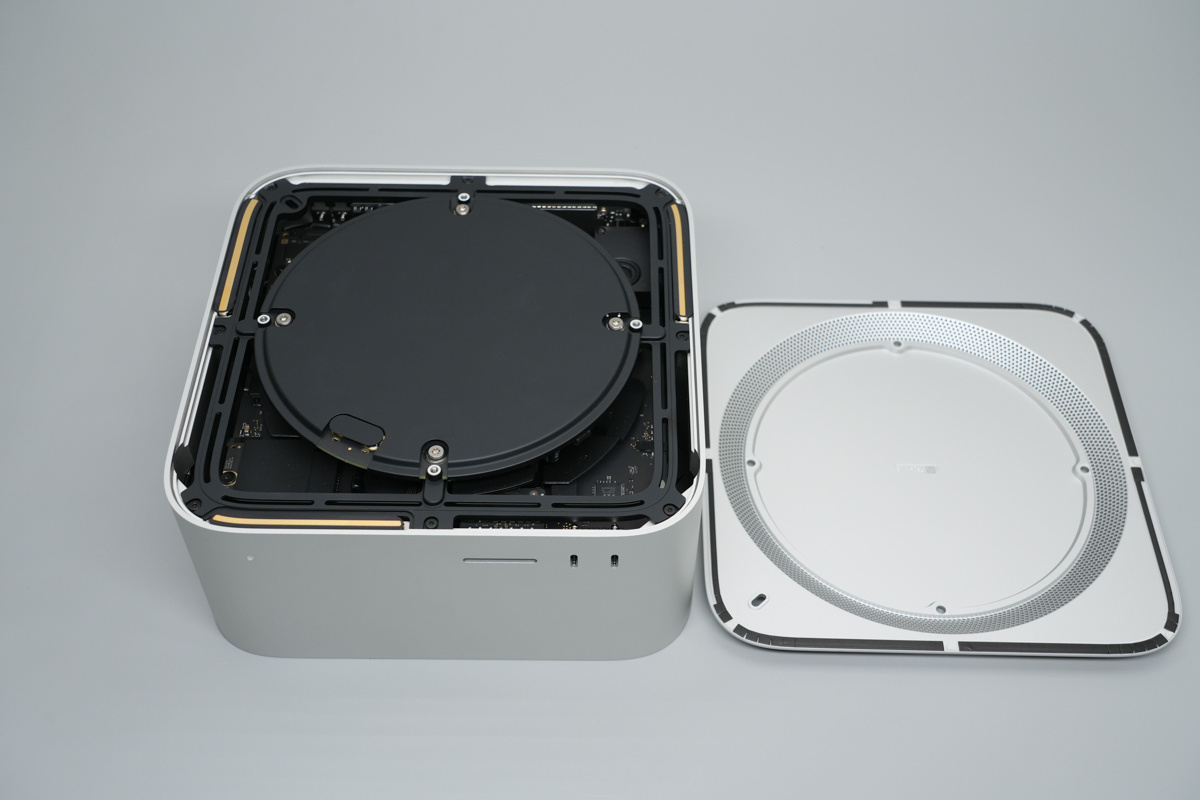
Remove the mounting screws and take off the bottom cover.
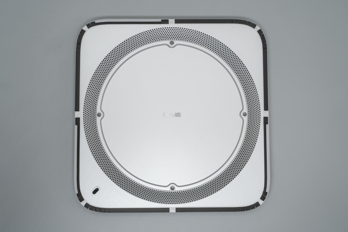
The bottom cover features mounting holes and ventilation openings, with conductive fabric applied along the edges for shielding.
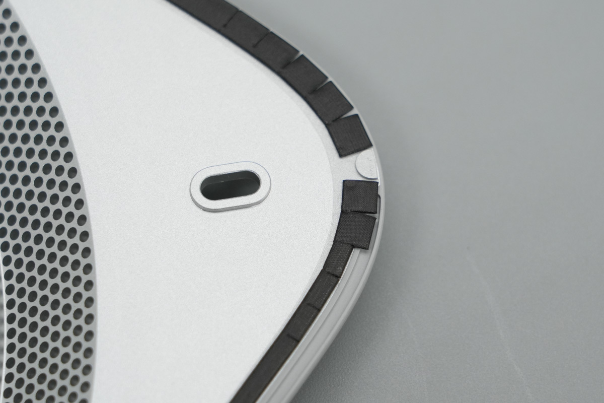
The conductive fabric along the edges.
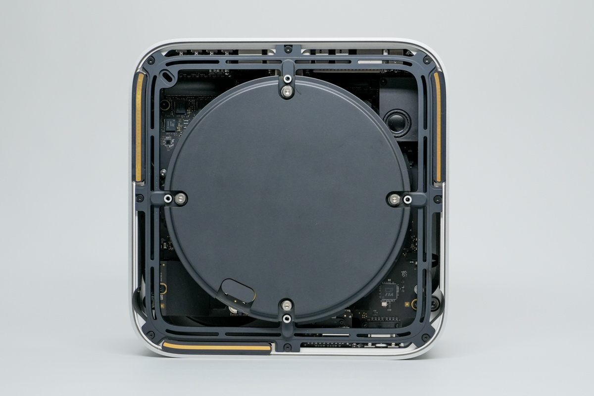
A circular power supply module is located in the center of the chassis, with mounting brackets and Wi-Fi antennas around the perimeter.
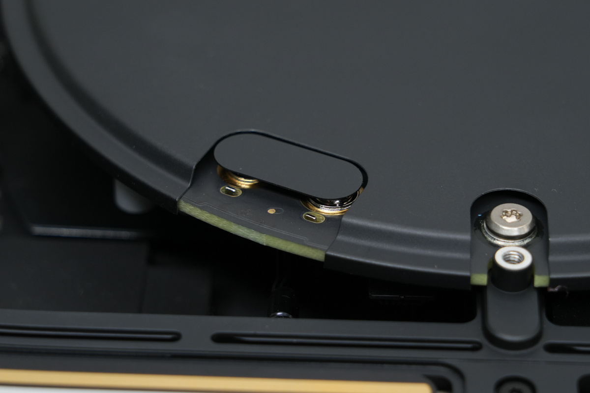
The power supply module is secured to the perimeter frame with screws. Mylar insulating sheets cover the positive and negative output terminals.
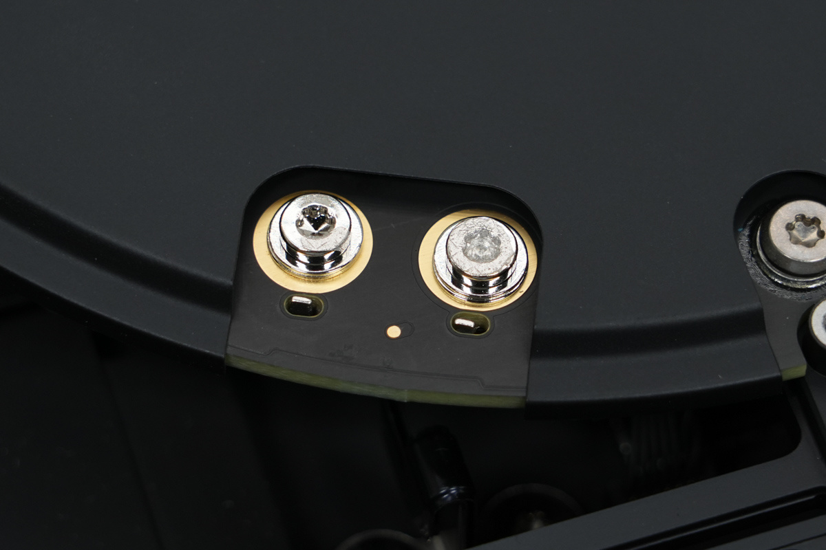
Mounting screws are located beneath the insulating sheets.
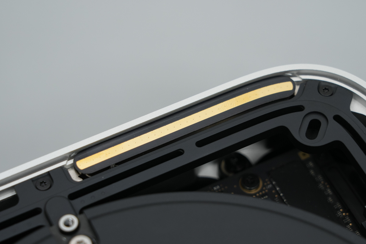
The Wi-Fi antenna.
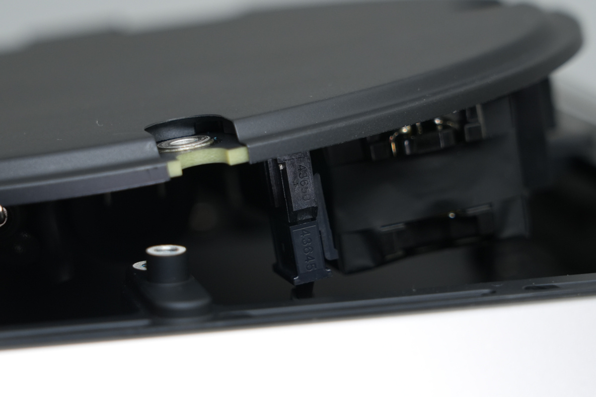
The power input cable connects to the power supply module through a connector.
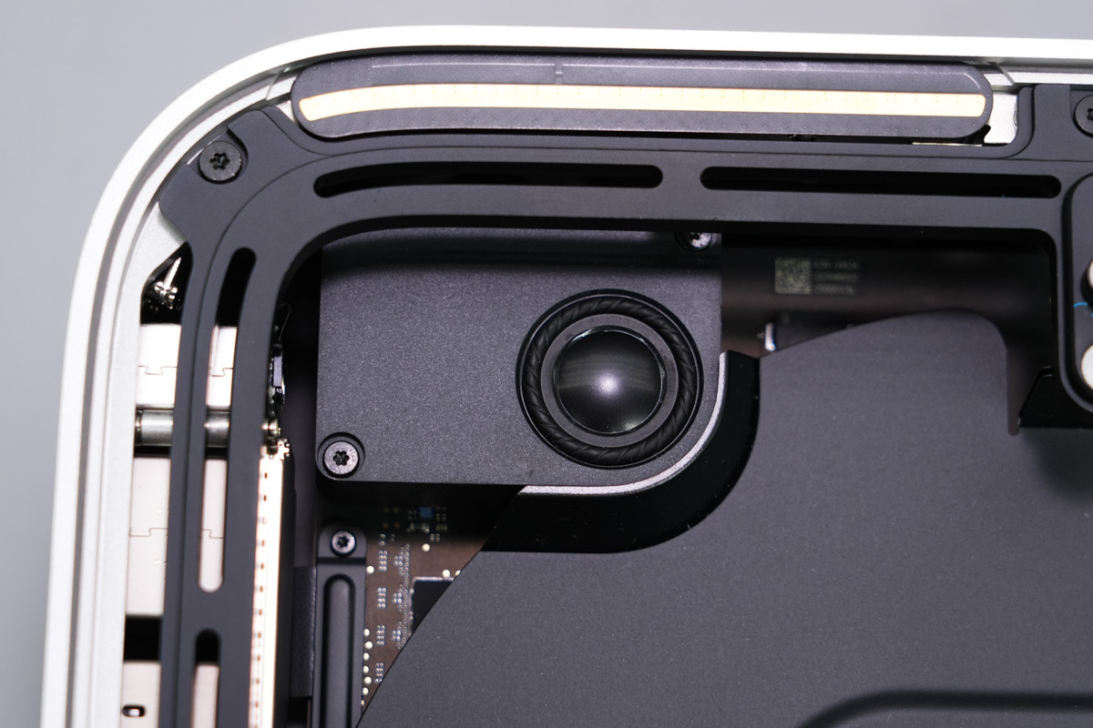
After removing the power supply module, a speaker can be found below.
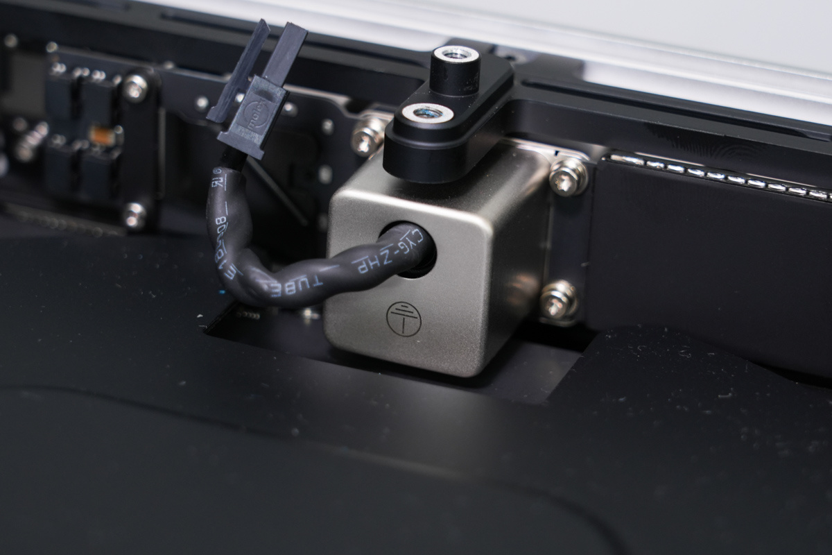
The AC input filter, which connects to the power supply module via wires.
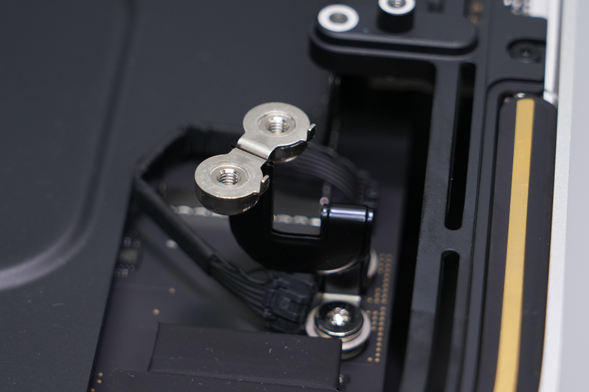
The logic board connects to the power supply module through a cable.
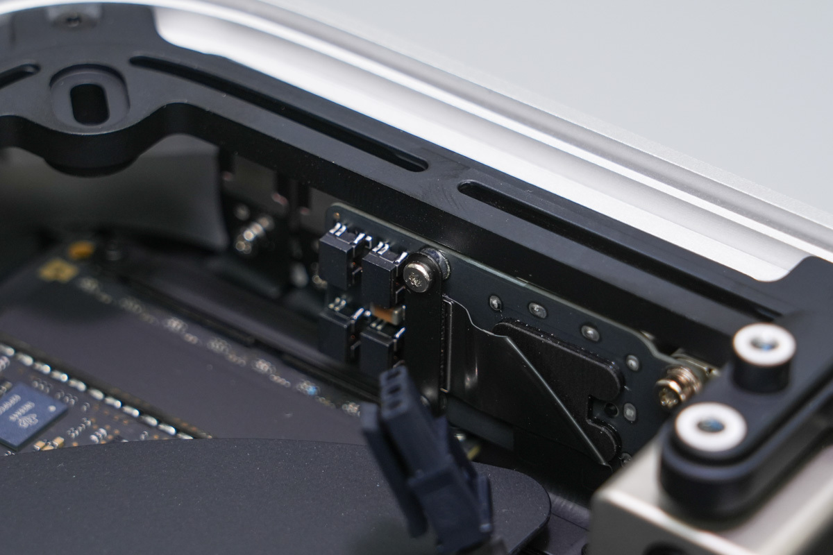
The 10Gb Ethernet port is secured inside the chassis with screws.
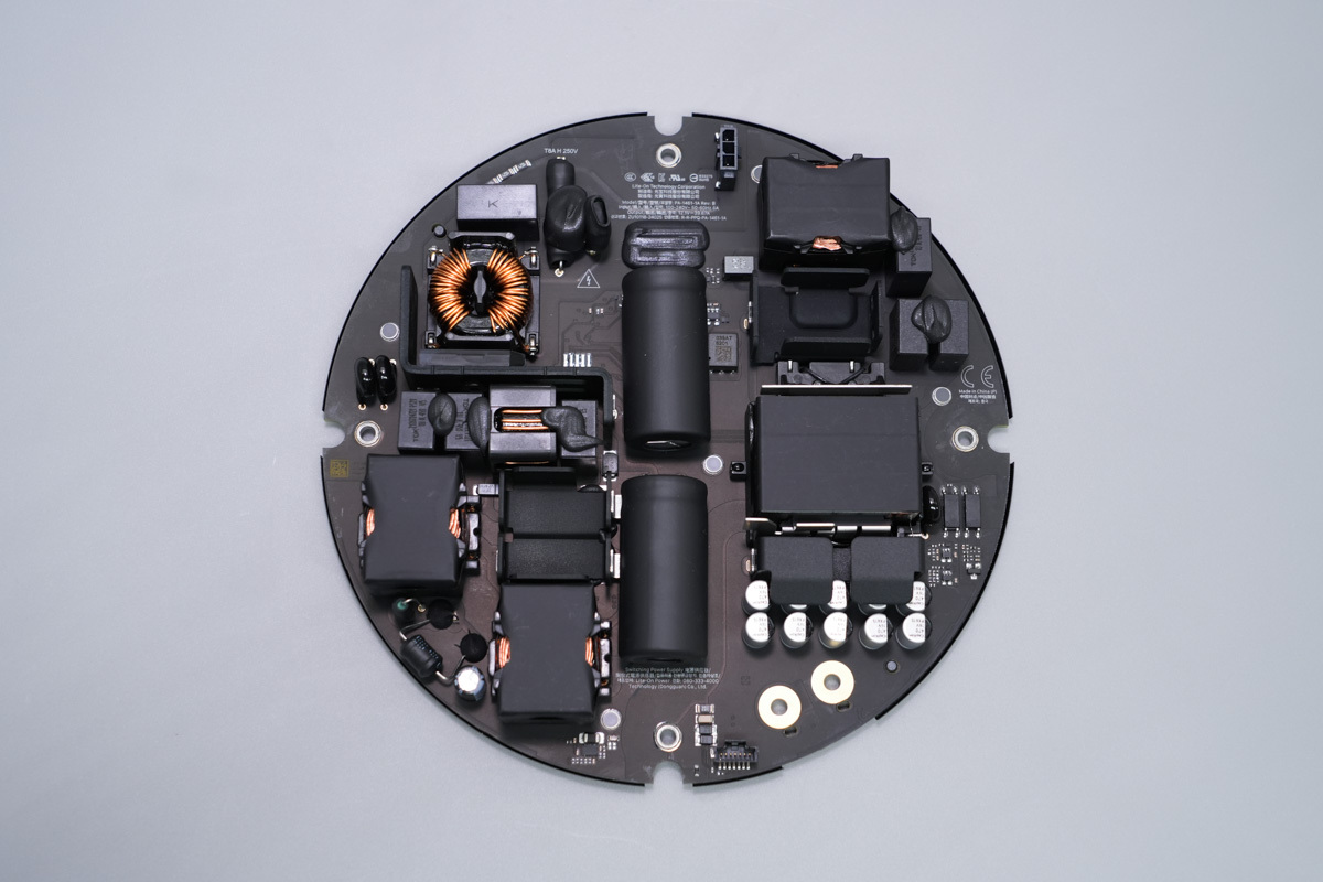
The front of the power supply module: the upper section contains the AC power inlet, fuse, varistor, X2 safety cap, and common-mode choke. The lower section contains the bridge rectifier, film filter cap, filter inductor, and PFC boost inductors. The high-voltage filter caps are located in the center and insulated with heat-shrink tubing.
The right side features the LLC resonant inductor and resonant caps, with the LLC transformer and solid-state filter caps below. The PFC switching MOSFETs, PFC rectifier MOSFETs, LLC switching MOSFETs, and synchronous rectifier MOSFETs are all covered by heatsinks. The power supply module uses two PFC boost inductors in an interleaved configuration.
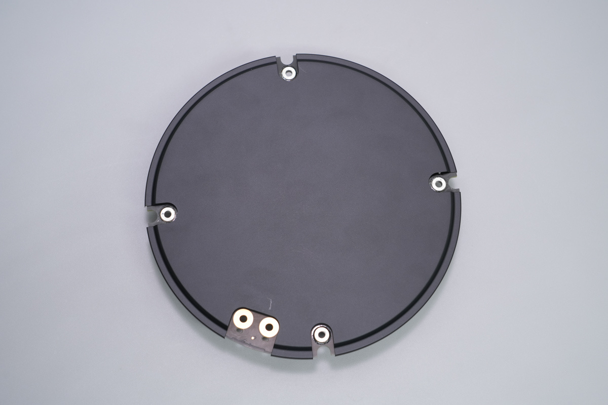
The back of the power supply module is covered with an insulating plate.
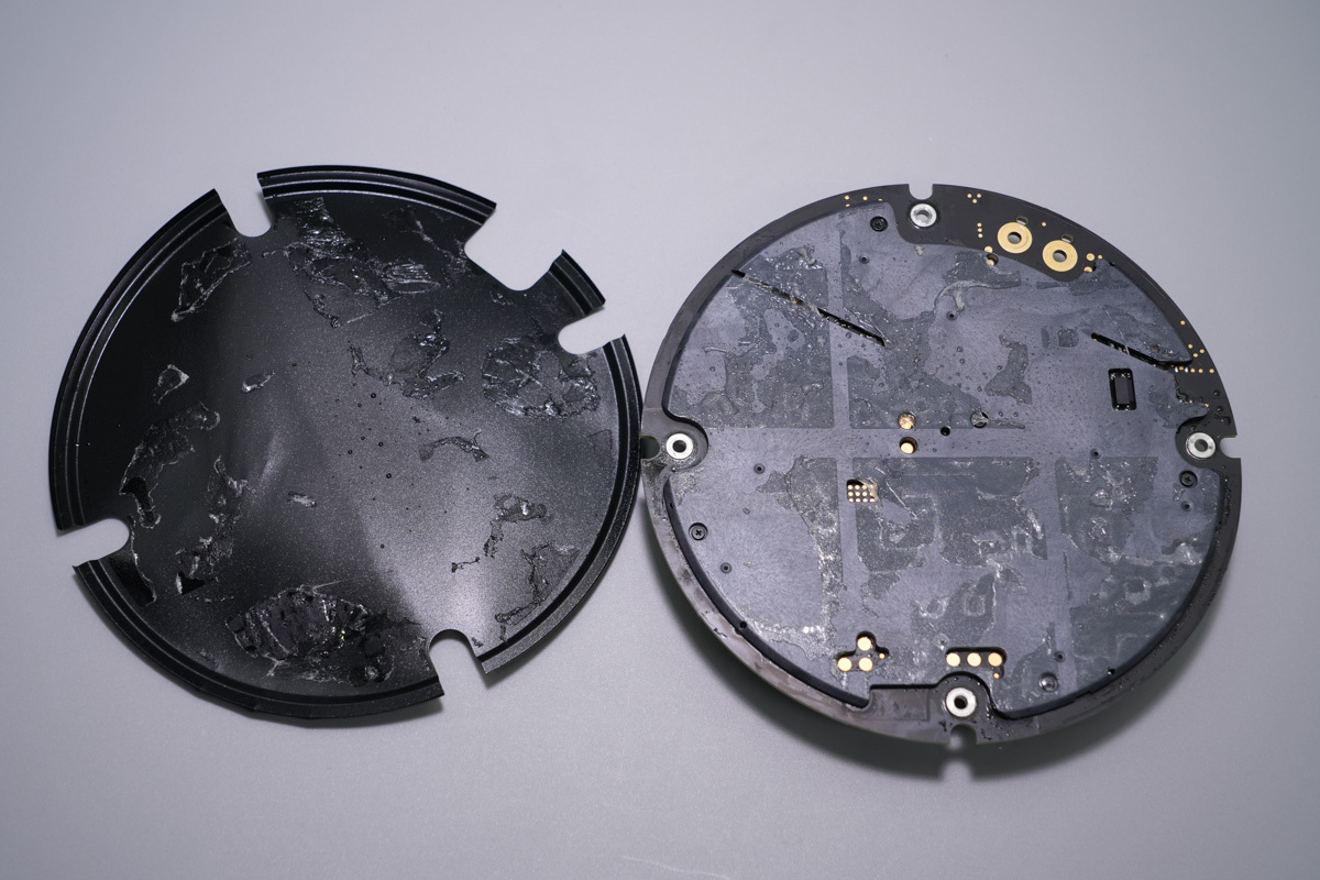
A plastic cover is located underneath the insulating plate.
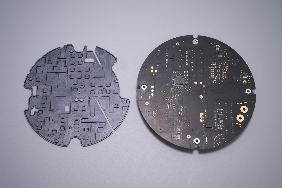
After removing the plastic cover, supporting structures can be seen on its underside, corresponding to the PCBA module.
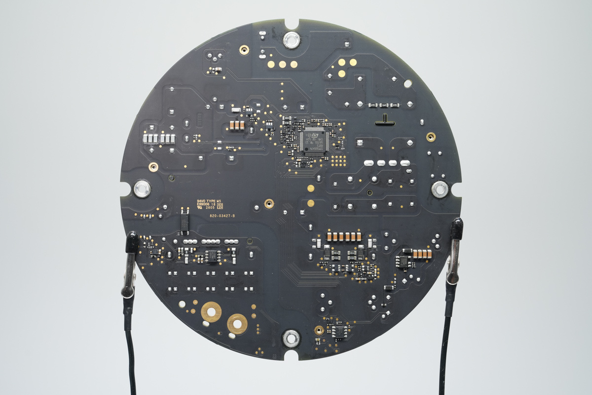
The back of the PCBA module: the right side features an MCU, while the left side contains the LLC gate driver. The lower-right section houses the PFC gate driver and a non-isolated buck converter. The lower-left section contains the synchronous rectifier driver.
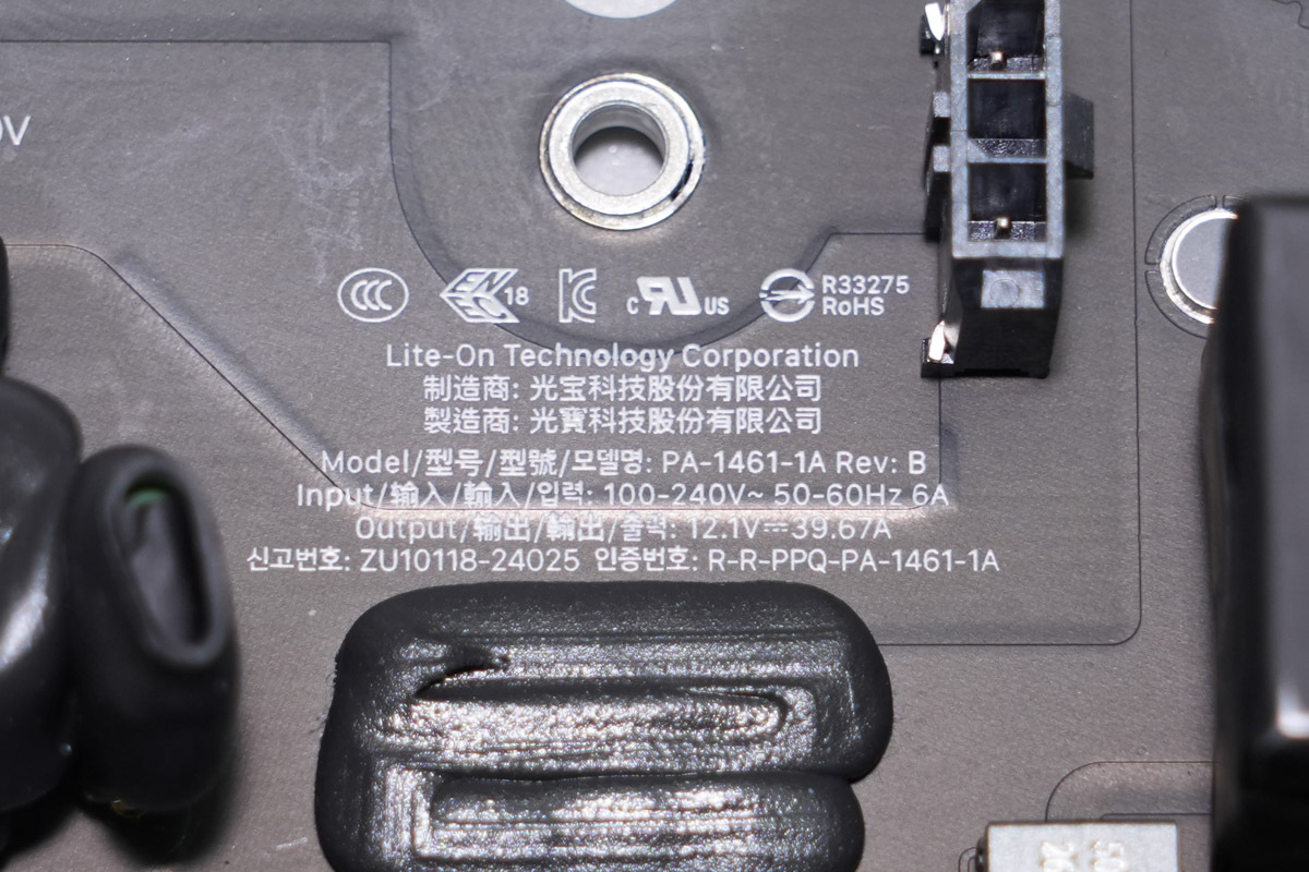
The power supply module is from LITEON, model PA-1461-1A. Its input rating is 100–240V~ 50–60Hz 6A, and its output rating is 12.1V DC, 39.67A, with a total output power of 480W.
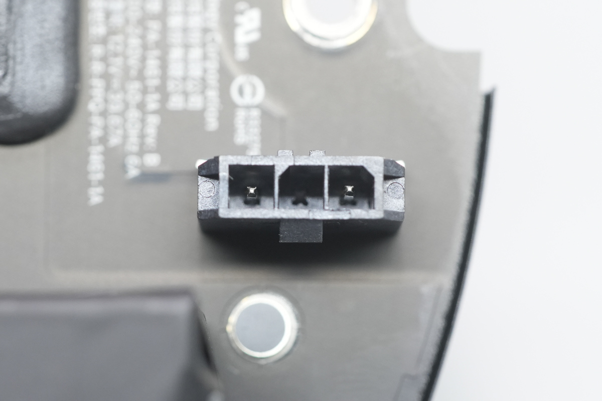
The AC input socket, which features a keyed design to prevent incorrect insertion.
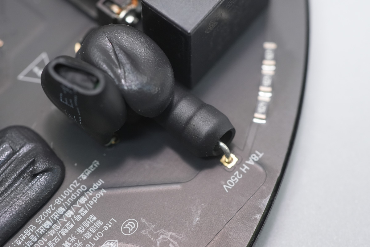
The fuse is covered with heat-shrink tubing for insulation and is rated at T8A 250V.
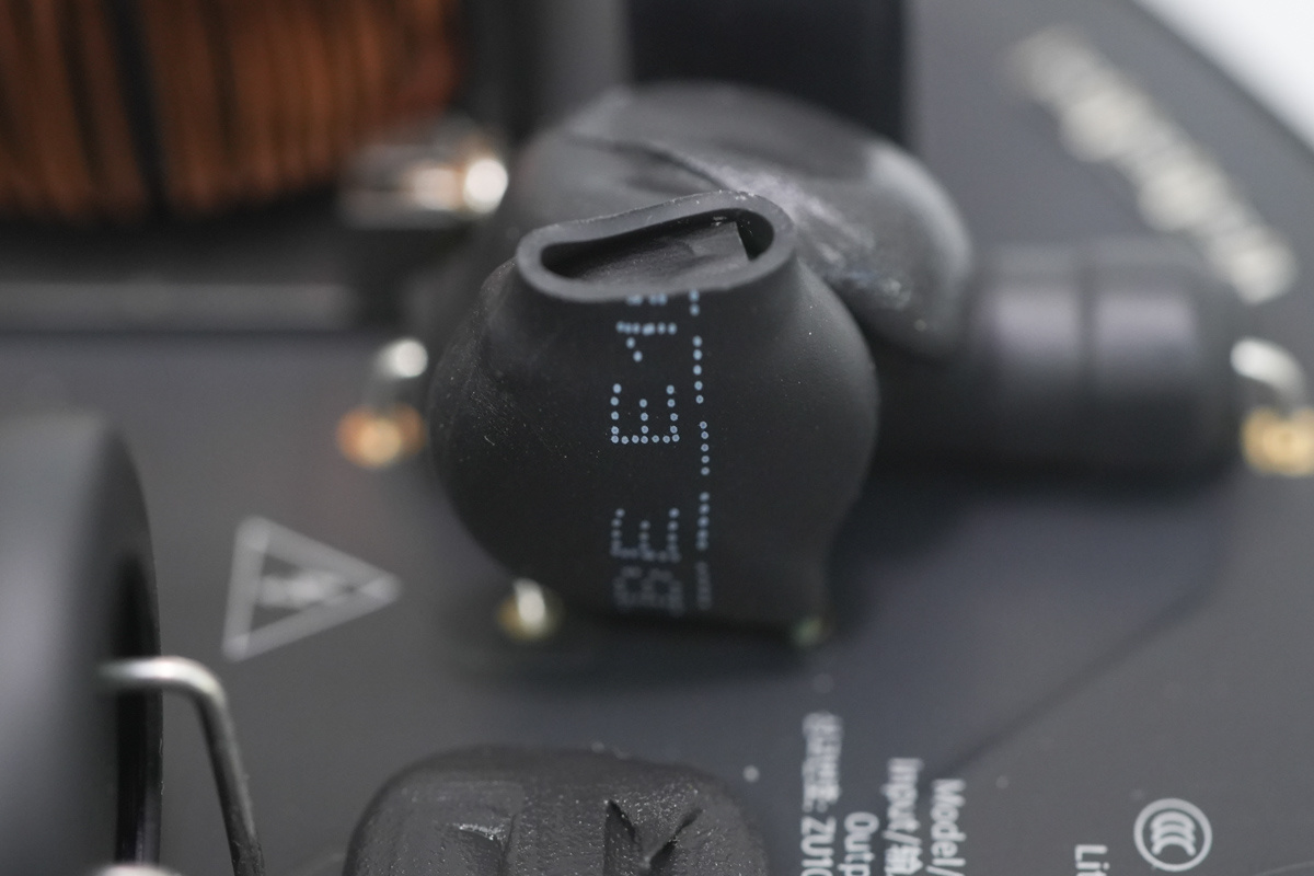
The thermistor is covered with heat-shrink tubing for insulation.
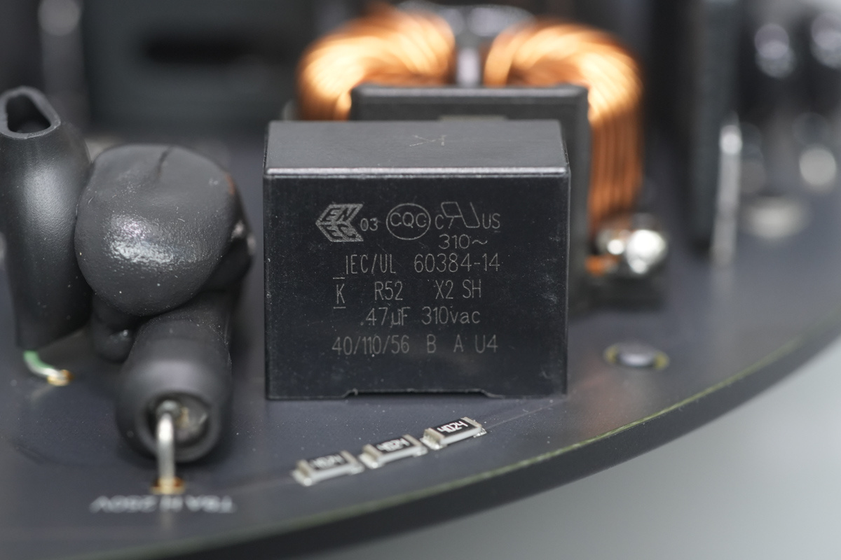
The X2 safety capacitor is from KEMET and rated at 0.47μF.
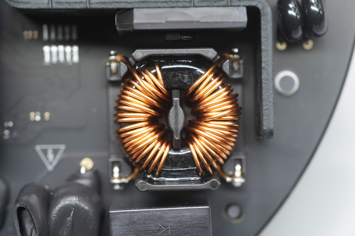
The common-mode choke features an insulating plastic frame.
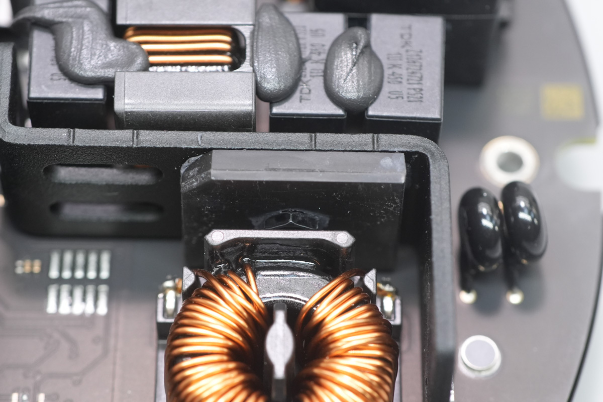
The bridge rectifier is equipped with a heatsink.
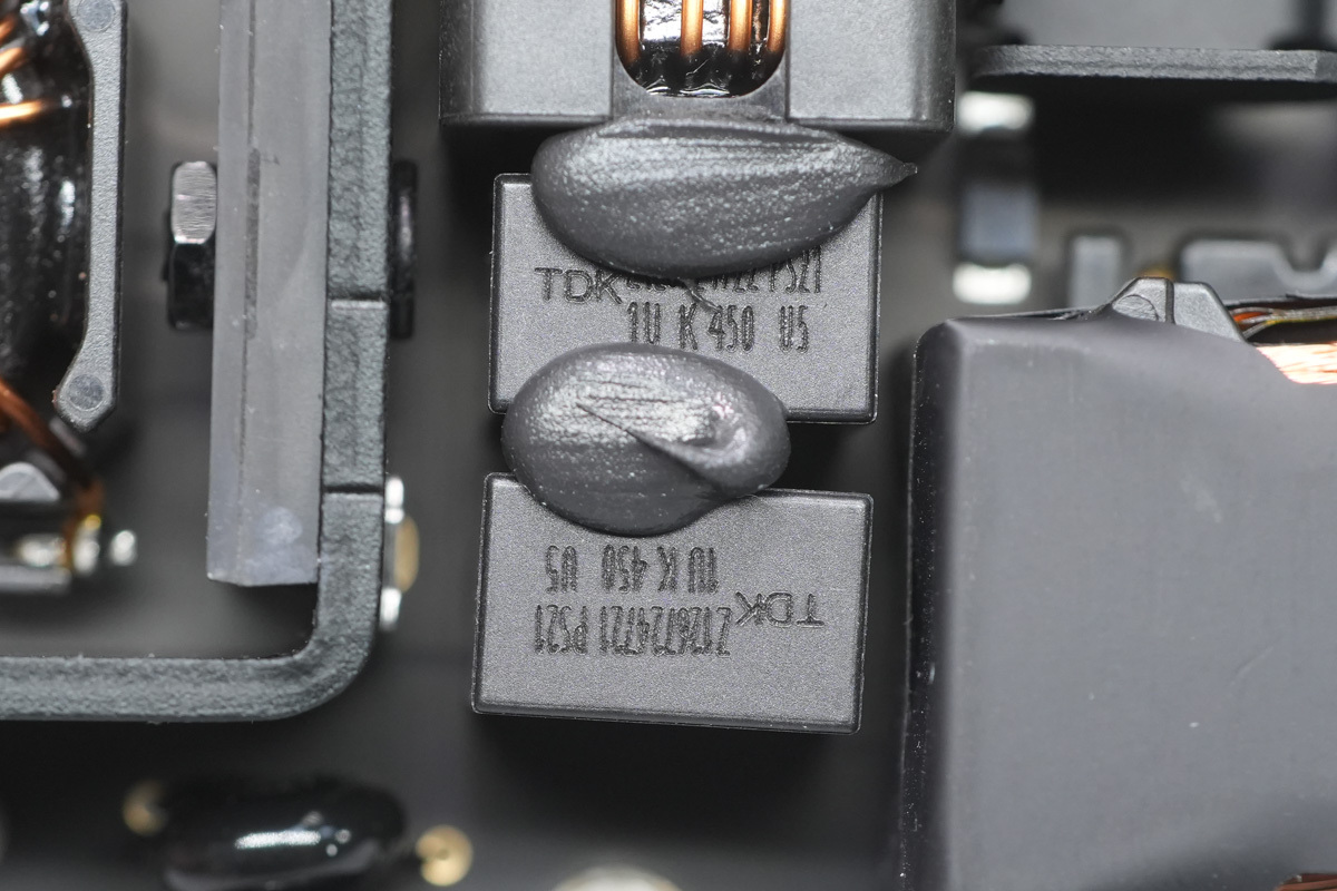
The filter cap is from TDK and rated at 1μF 450V.
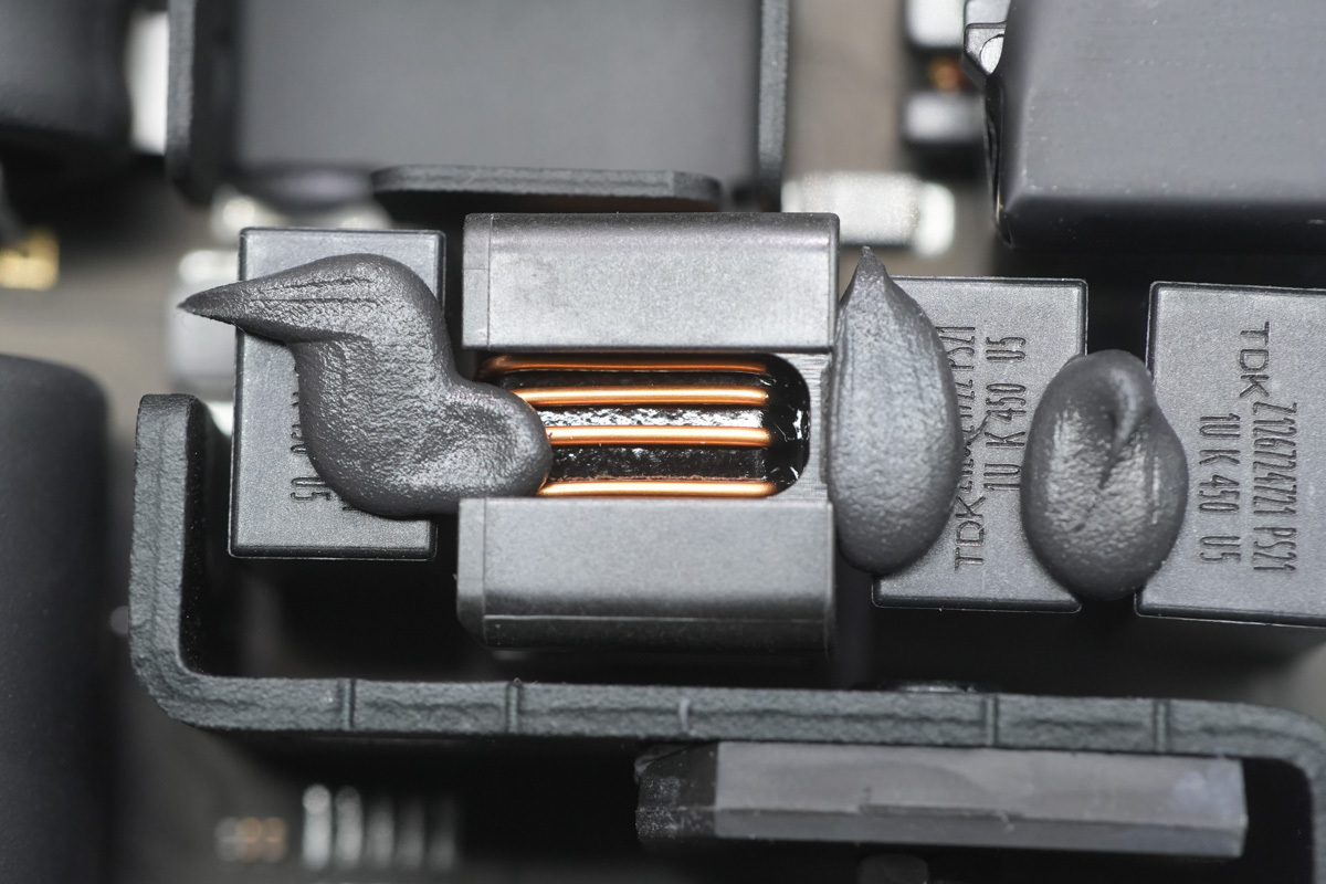
The filter inductor is wound with enameled wire and enclosed in a plastic housing for insulation.
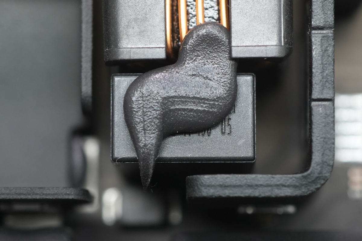
Another filter cap.
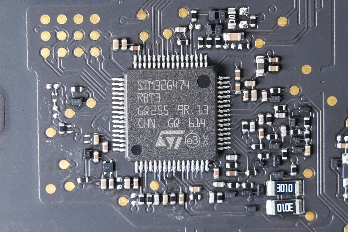
The main control MCU is from ST, model STM32G474RBT3. It integrates an ARM Cortex-M4 core running at 170MHz, an FPU and DSP, 128KB of Flash memory, and 128KB of SRAM. It also features standard and advanced communication interfaces and is housed in an LQFP-64 package.
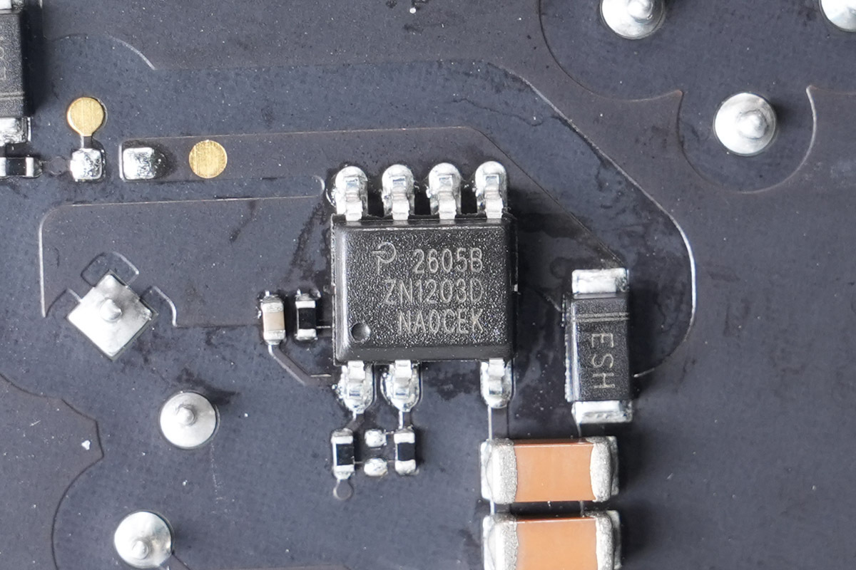
The buck converter chip is from PI, model ZN1203D, housed in an SO-8C package.
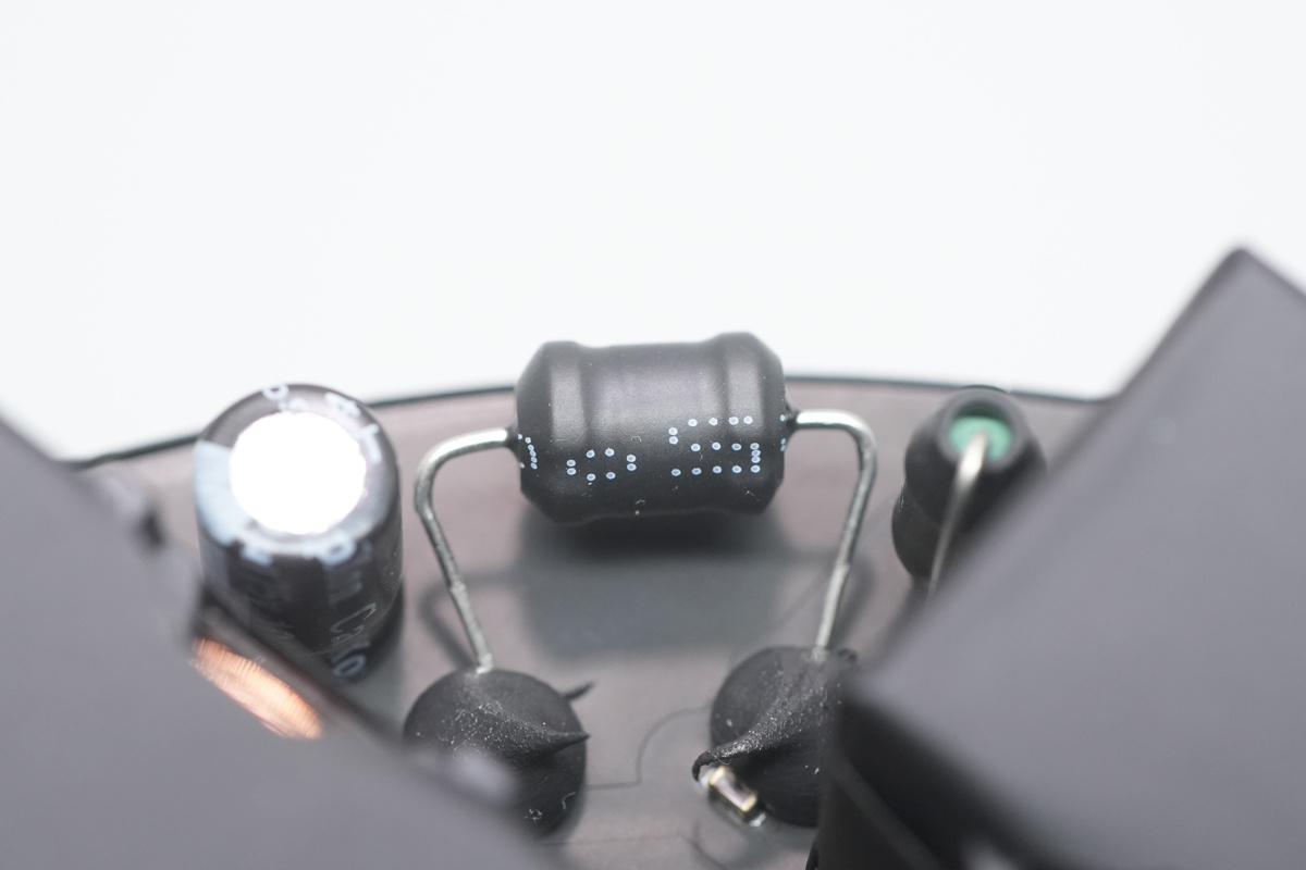
The buck inductor is covered with heat-shrink tubing for insulation.
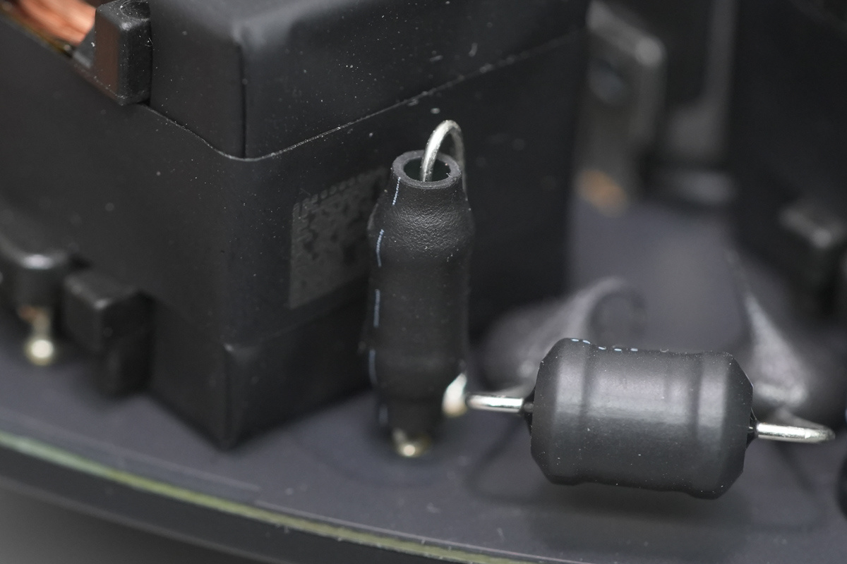
Another inductor is covered with heat-shrink tubing for insulation.
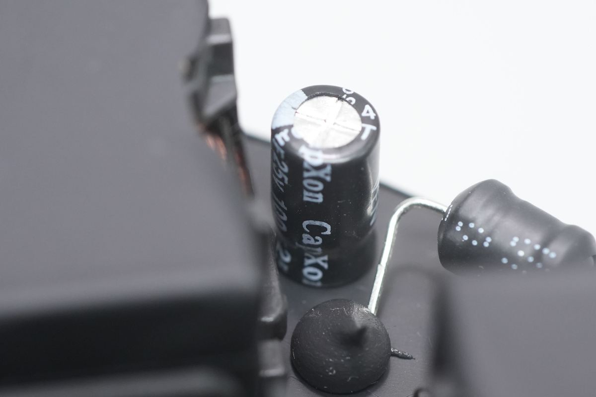
The filter cap is from CapXon and rated at 100μF 25V.
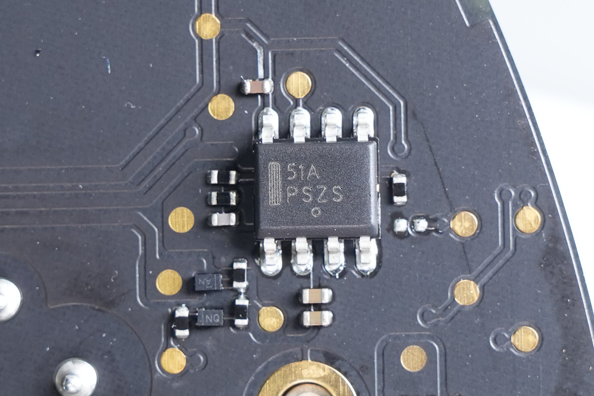
The voltage regulator is from onsemi, marked 51A, model NCV2951. It supports an input voltage of up to 30V, an adjustable output voltage from 1.25V to 29V, and an output current of 100mA. It is housed in an SOIC-8 package.
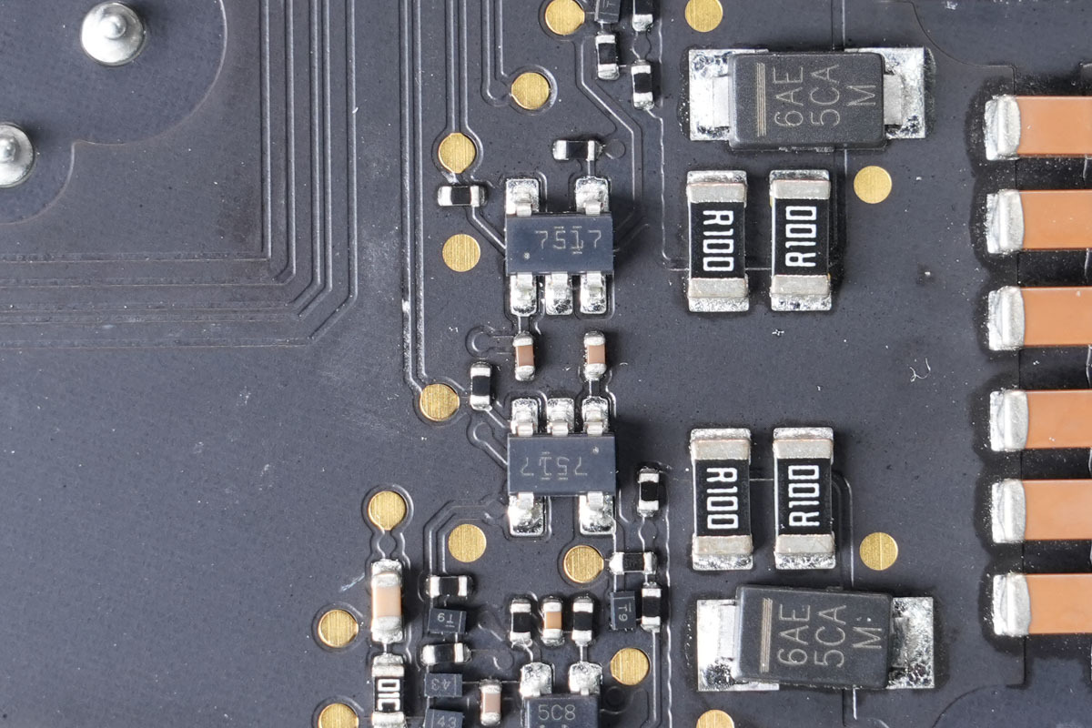
The gate driver is from TI, marked 7517, model UCC27517. It is a single-channel, high-speed, low-side gate driver supporting 4A source and sink currents and an operating voltage range of 4.5–18V. It is housed in a SOT-23 package. Two units are used to drive the interleaved PFC switching MOSFETs.
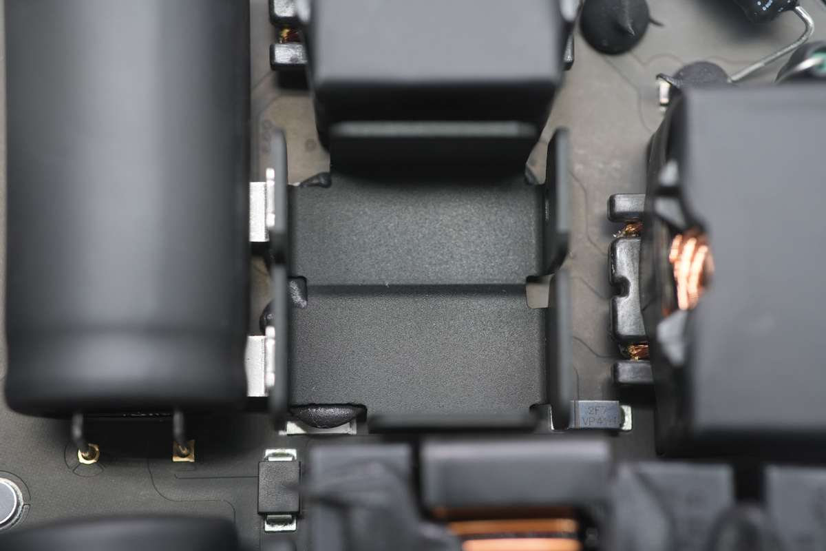
The PFC switching MOSFETs and PFC rectifier MOSFETs are located beneath the heatsink.
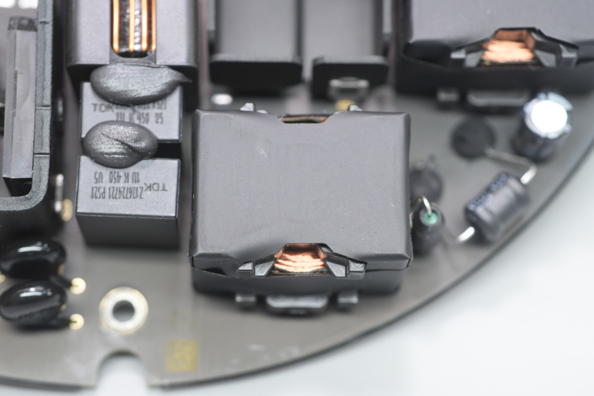
The PFC boost inductor is wound with litz wire.
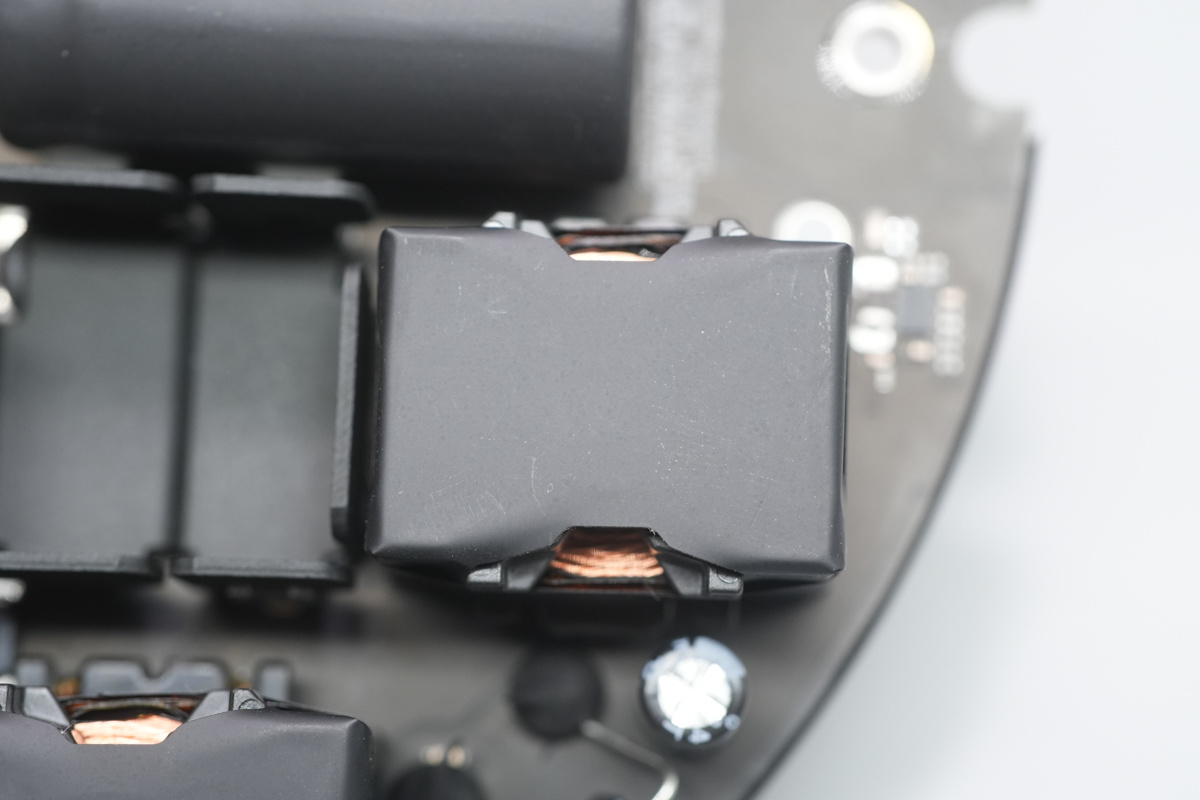
The other one shares the same specs.
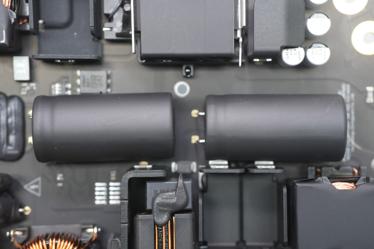
The high-voltage filter caps are covered with heat-shrink tubing for insulation.
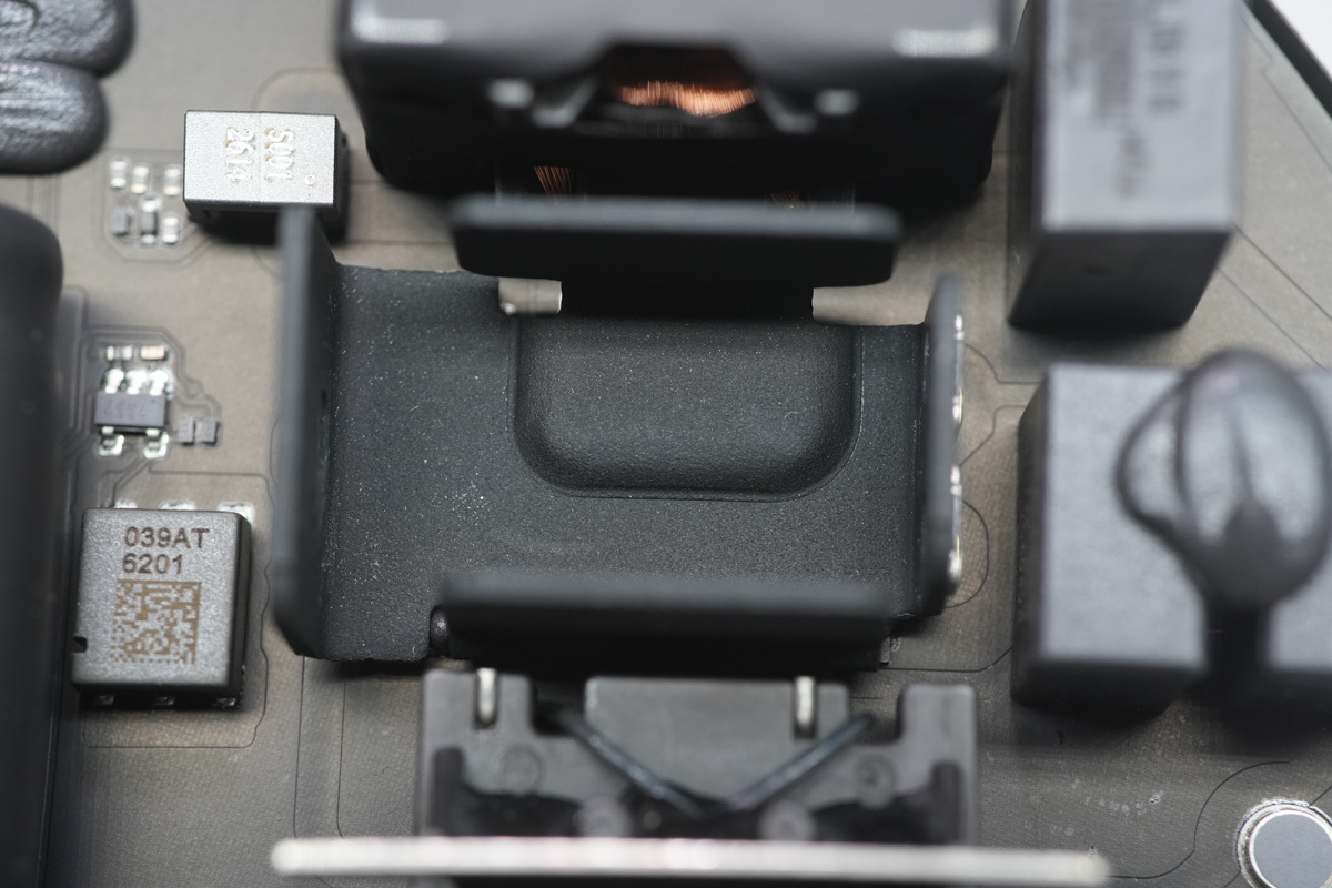
The LLC switching MOSFETs are located beneath the heatsink.
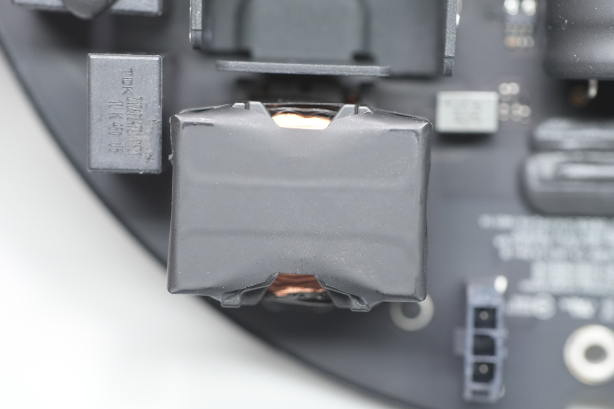
The resonant inductor is wound with litz wire.
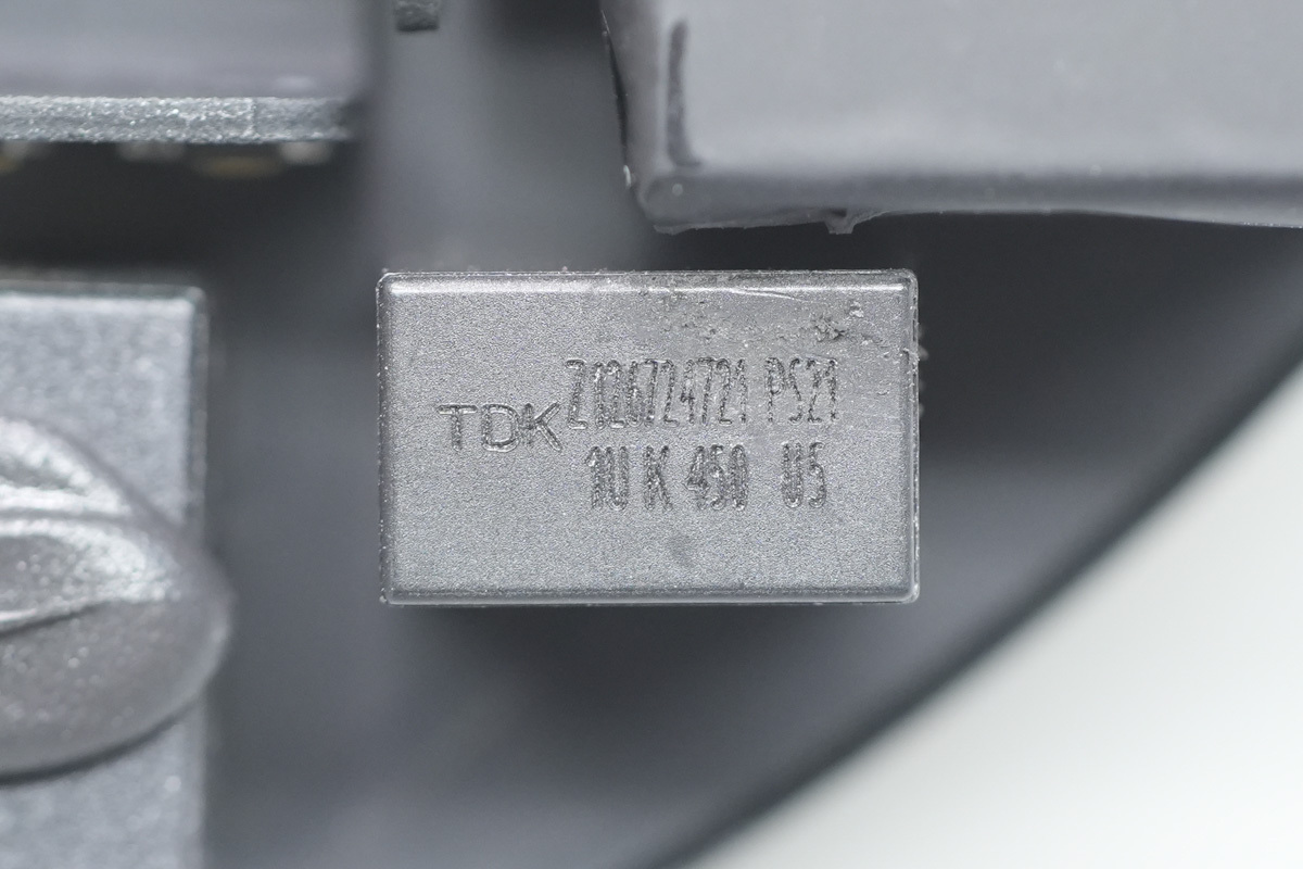
The film filter cap is rated at 1μF 450V.
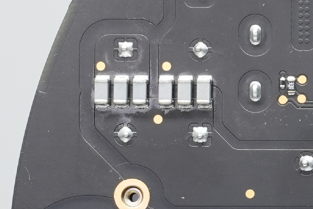
The SMD NPO resonant caps.
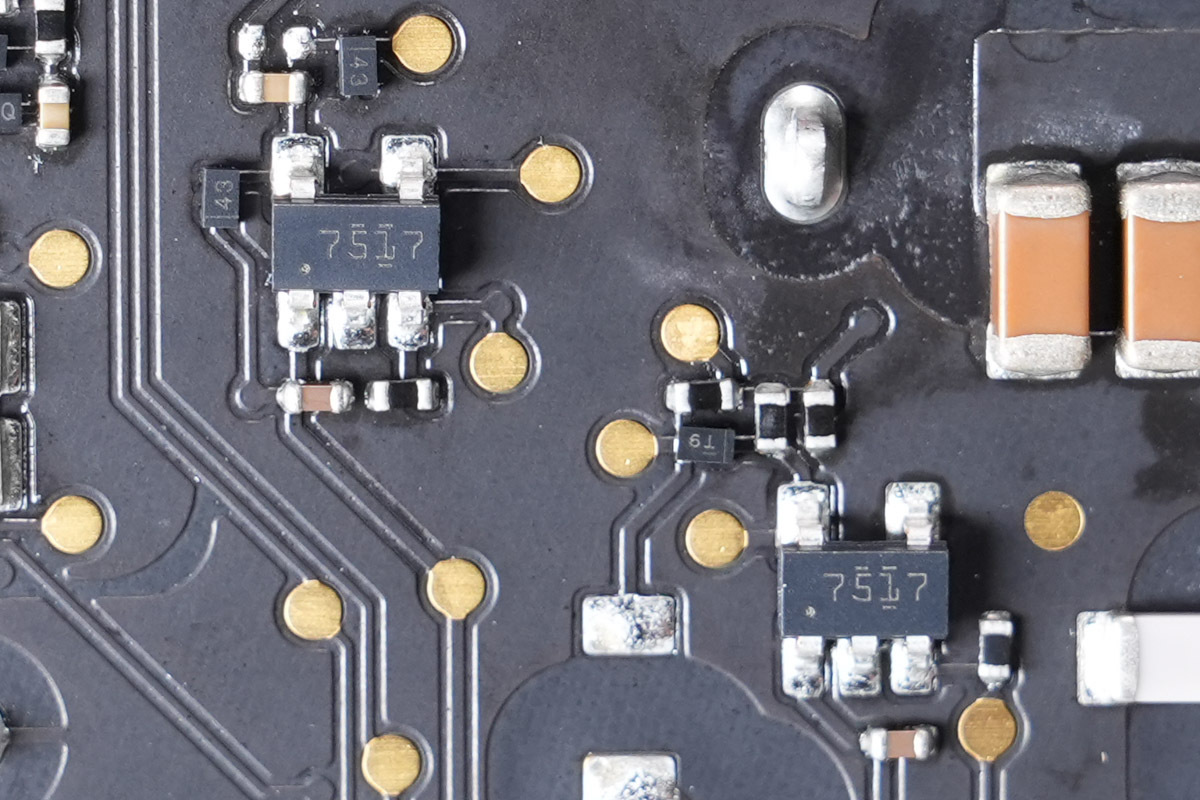
Two TI gate drivers, model UCC27517.
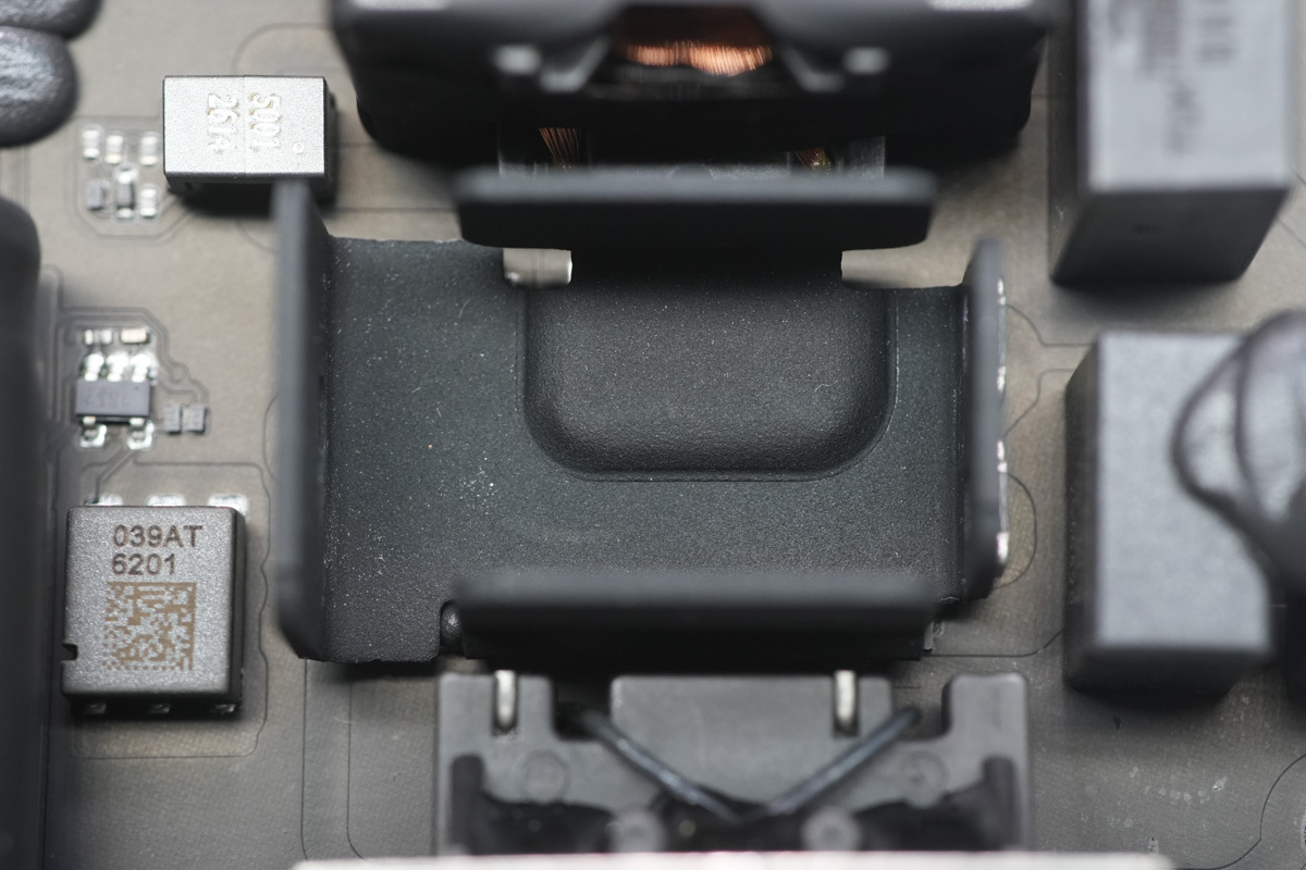
The LLC switching MOSFETs are equipped with a heatsink.
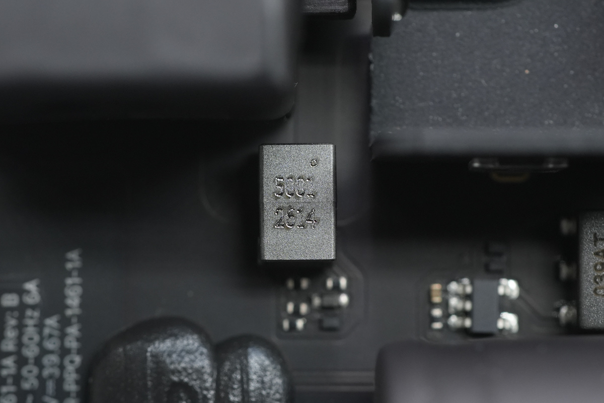
The current transformer used to detect switching MOSFET current.
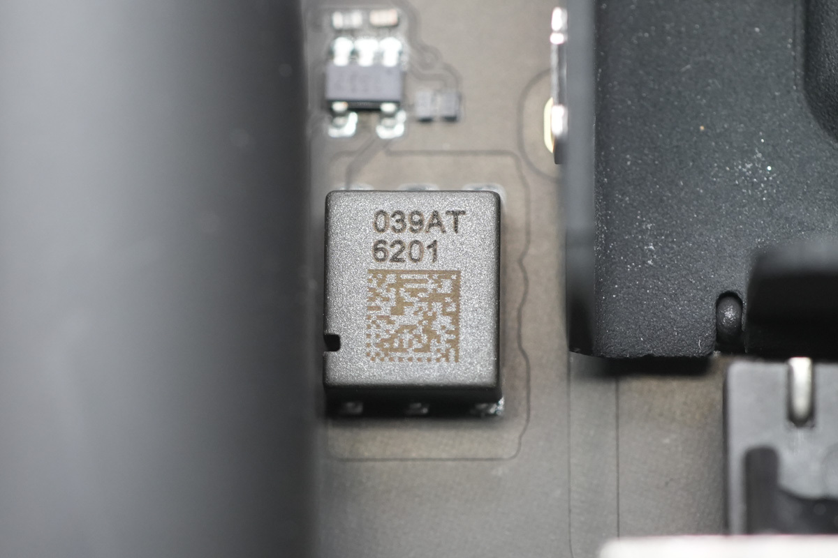
The isolated gate-drive transformer.
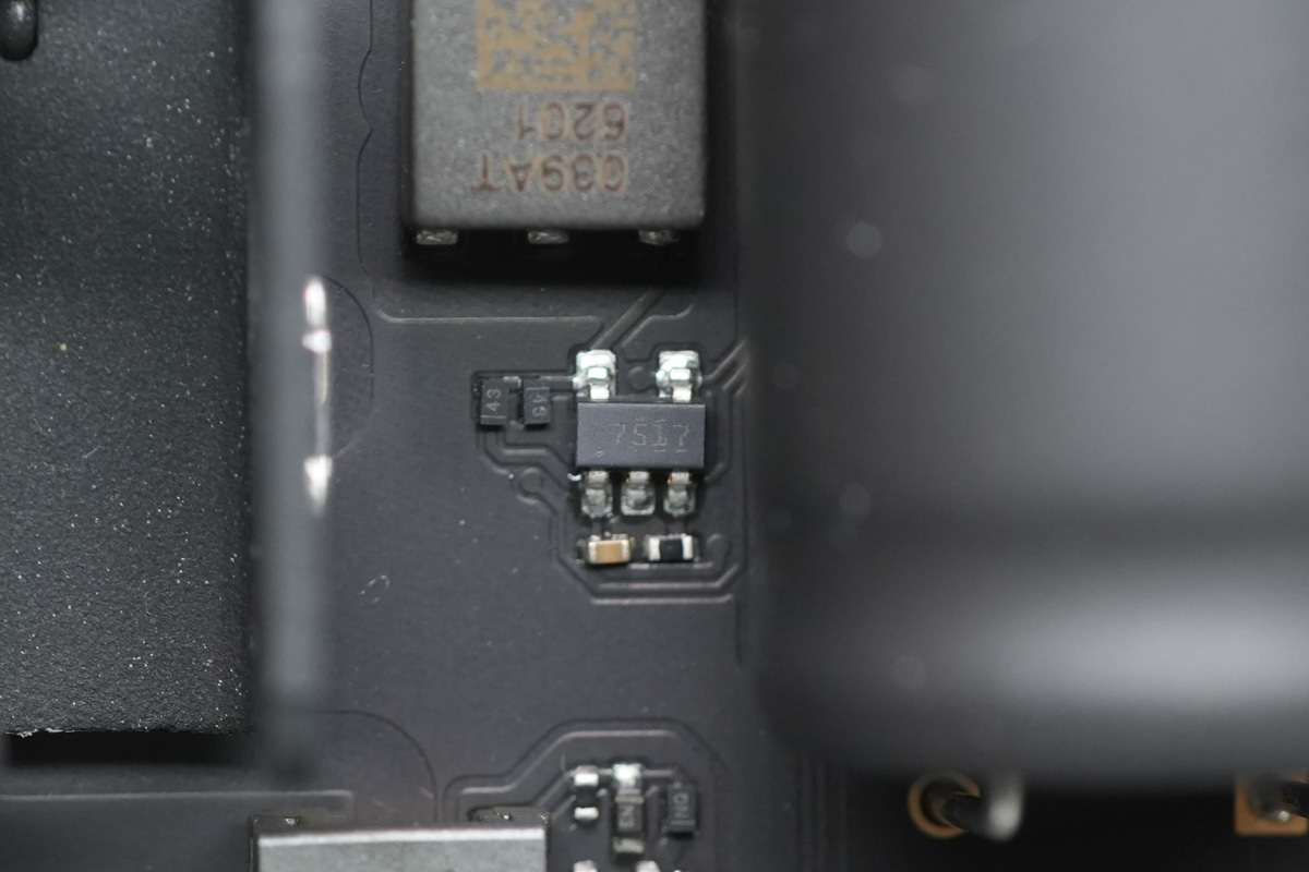
The gate driver is a TI UCC27517.
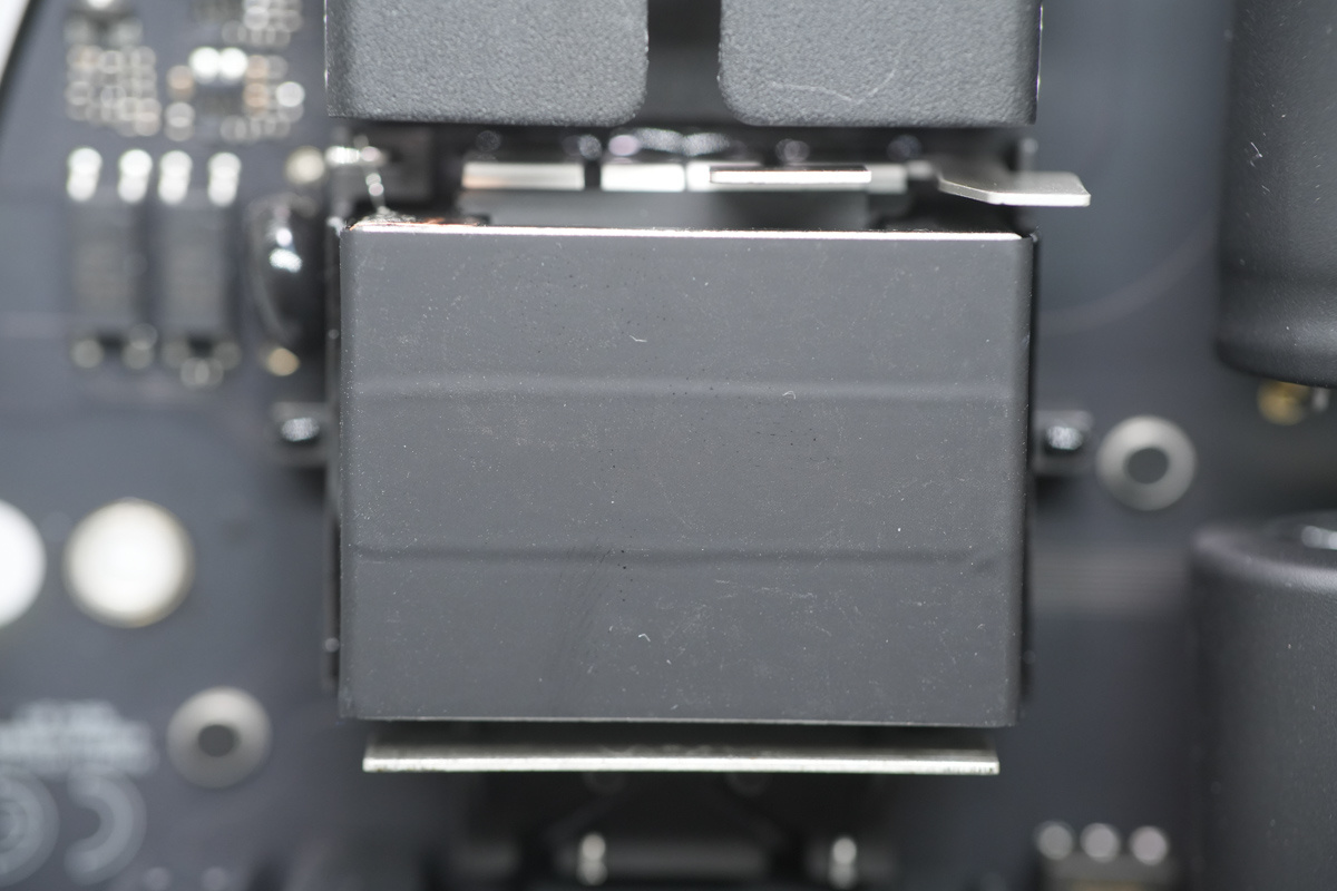
The LLC transformer.
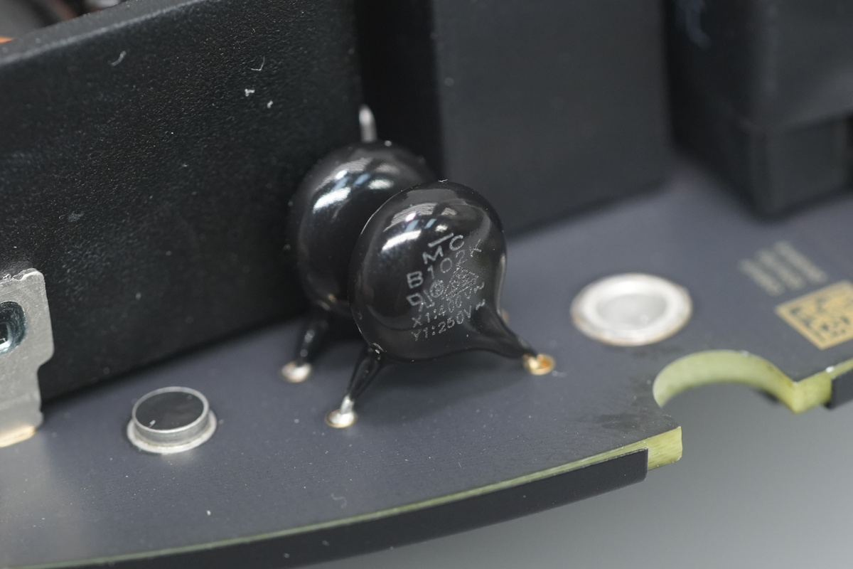
The Y-cap is marked B102K.
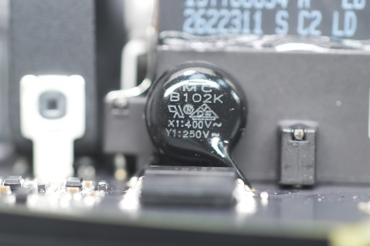
The other one shares the same model.
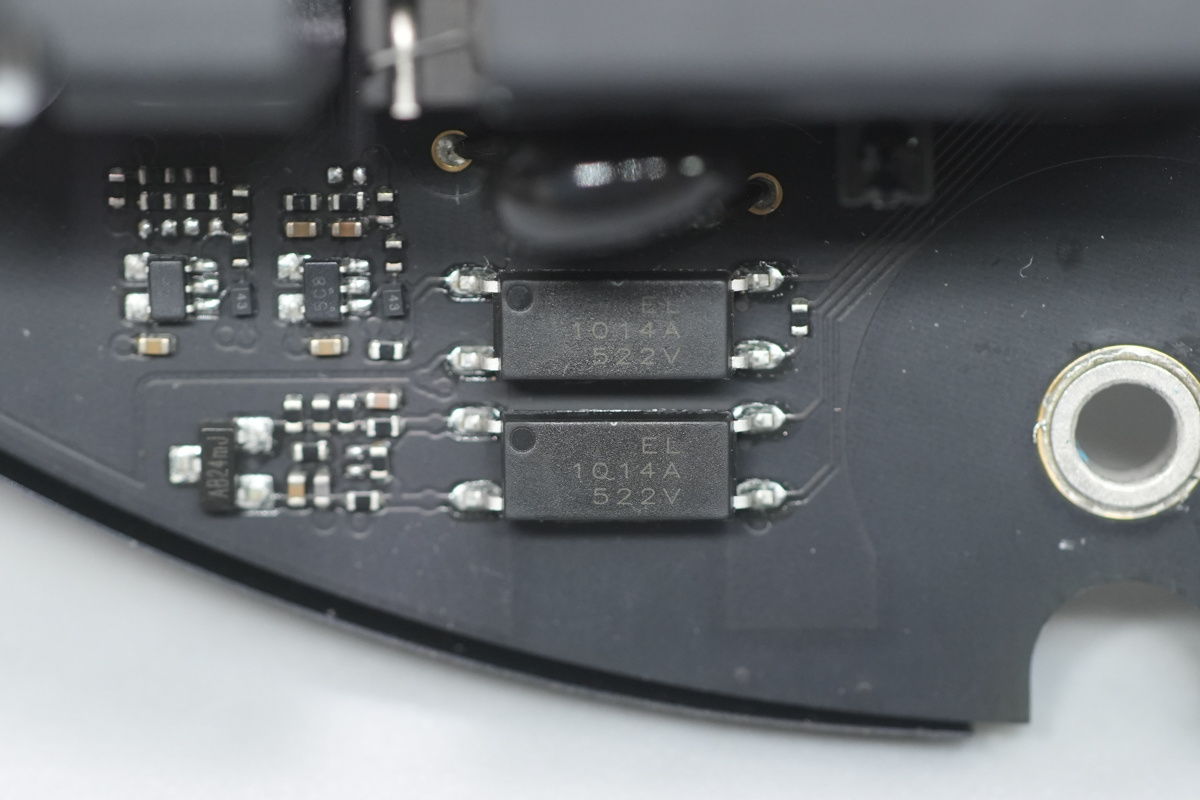
An Everlight EL1014K optocoupler is used for output voltage feedback and protection control.
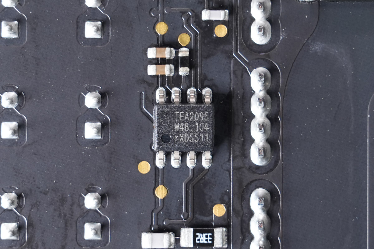
The synchronous rectification controller is from NXP, model TEA2095. It is a dual-channel synchronous rectification controller with two integrated drivers that can drive two synchronous rectifier MOSFETs simultaneously or operate independently. It is designed for LLC resonant power supplies and housed in an SO-8 package.
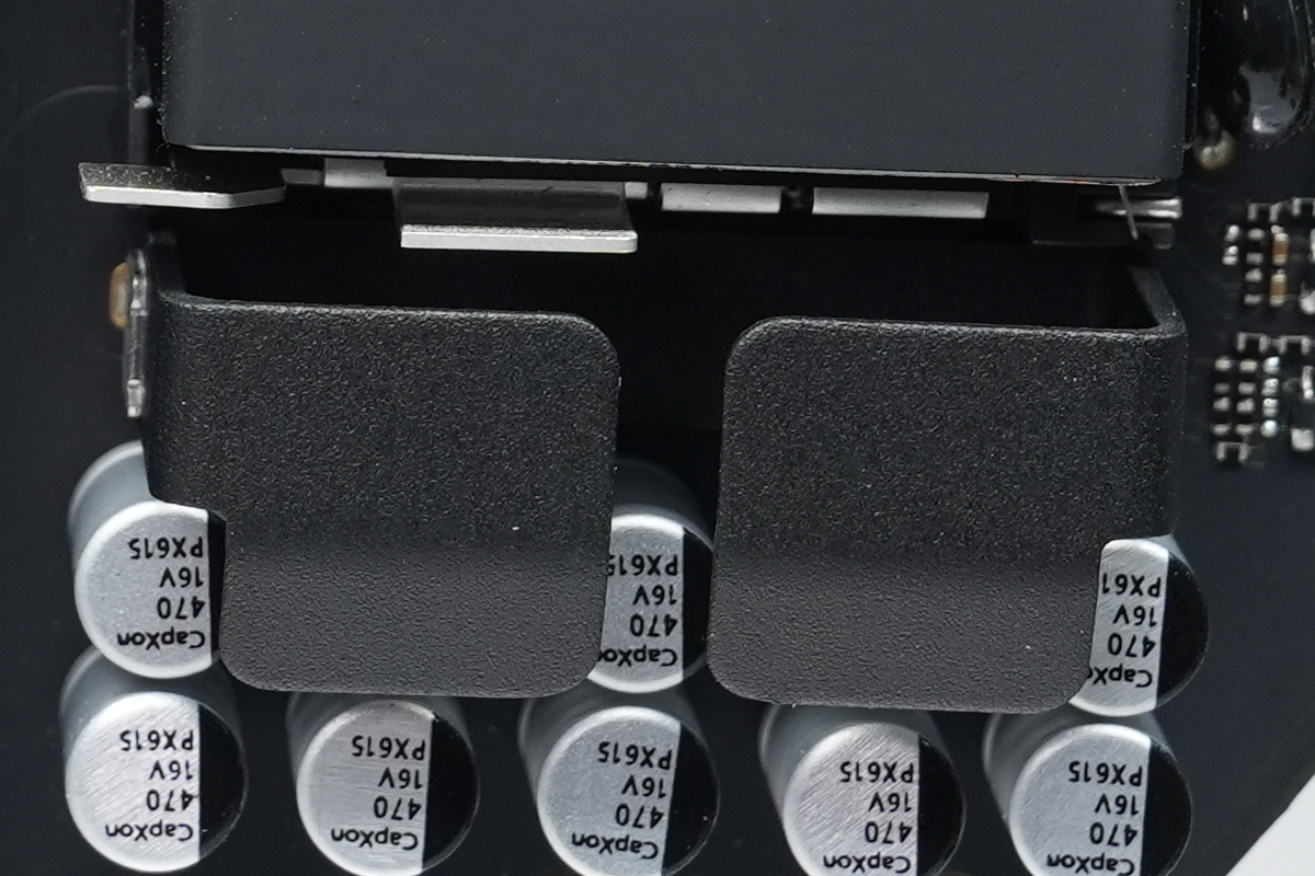
The synchronous rectifier MOSFETs are equipped with a heatsink.
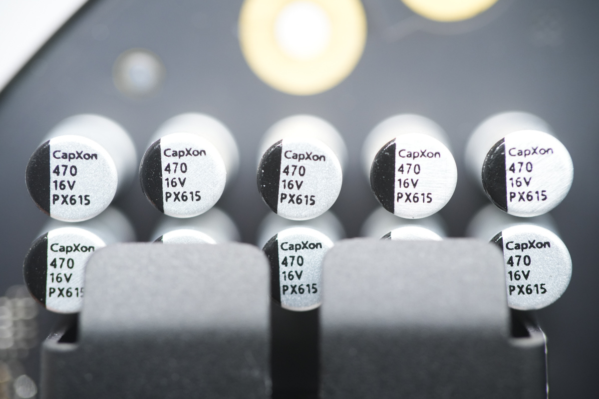
The filter caps are from CapXon, belonging to the PX series of solid-state caps, rated at 470μF 16V.
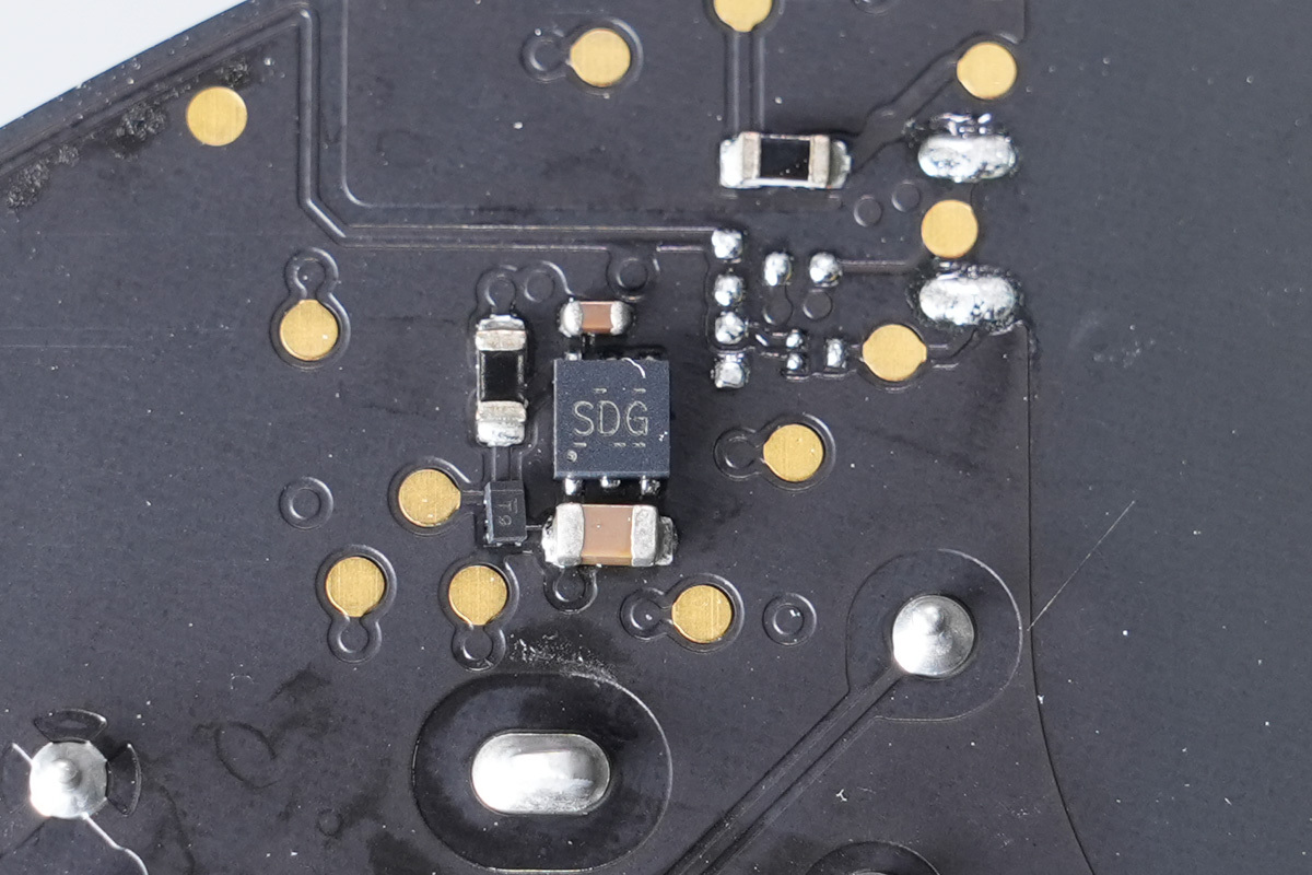
The voltage regulator is from TI, marked SDG, model TPS70933. It is a low-dropout regulator supporting a 30V input, a 3.3V output, and a 150mA output current, with a peak output current of 200mA. It features thermal shutdown and overcurrent protection and is housed in a WSON-6 package.
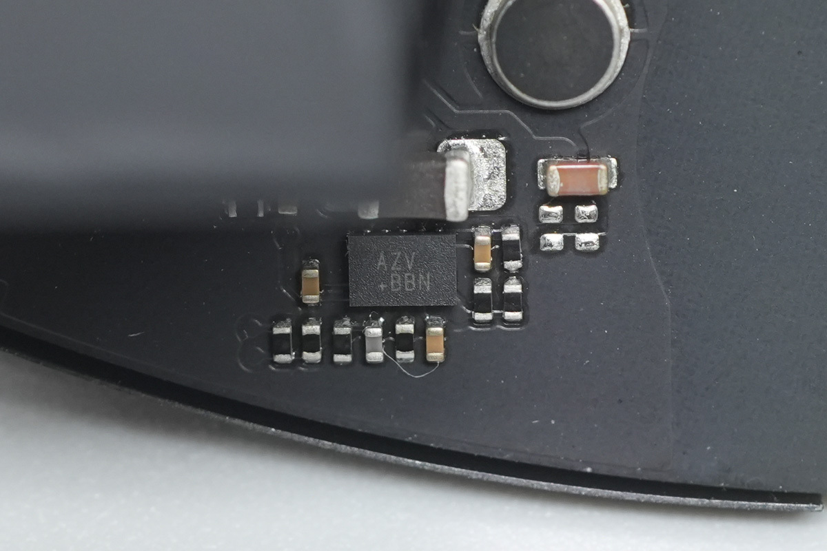
A chip, marked AZV.
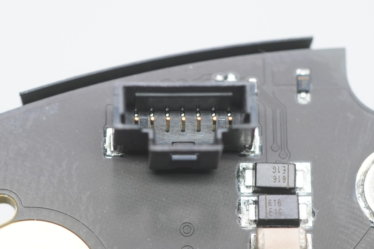
The power supply board features a connector.
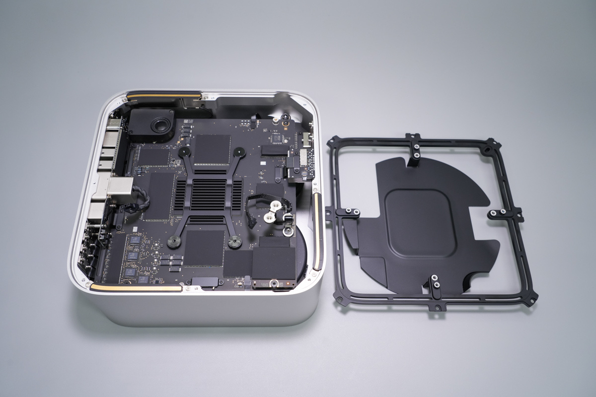
Remove the internal mounting bracket to continue the disassembly.
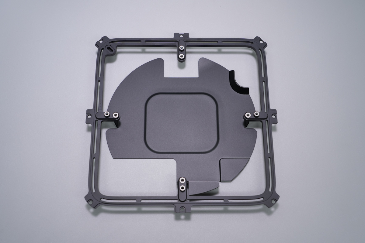
The bracket is made of aluminum alloy and features a shielding plate in the center.
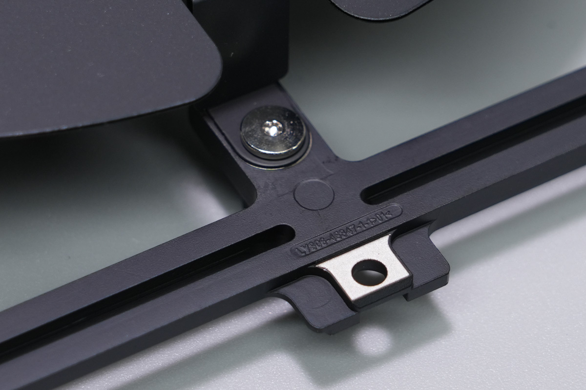
The shielding plate is secured to the frame with screws.
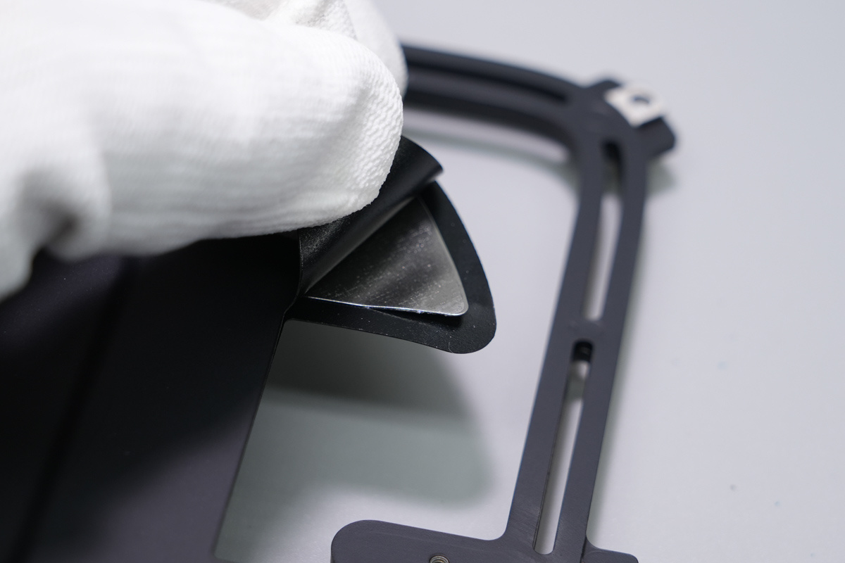
The shielding plate consists of an outer plastic insulating layer and an inner aluminum alloy layer.
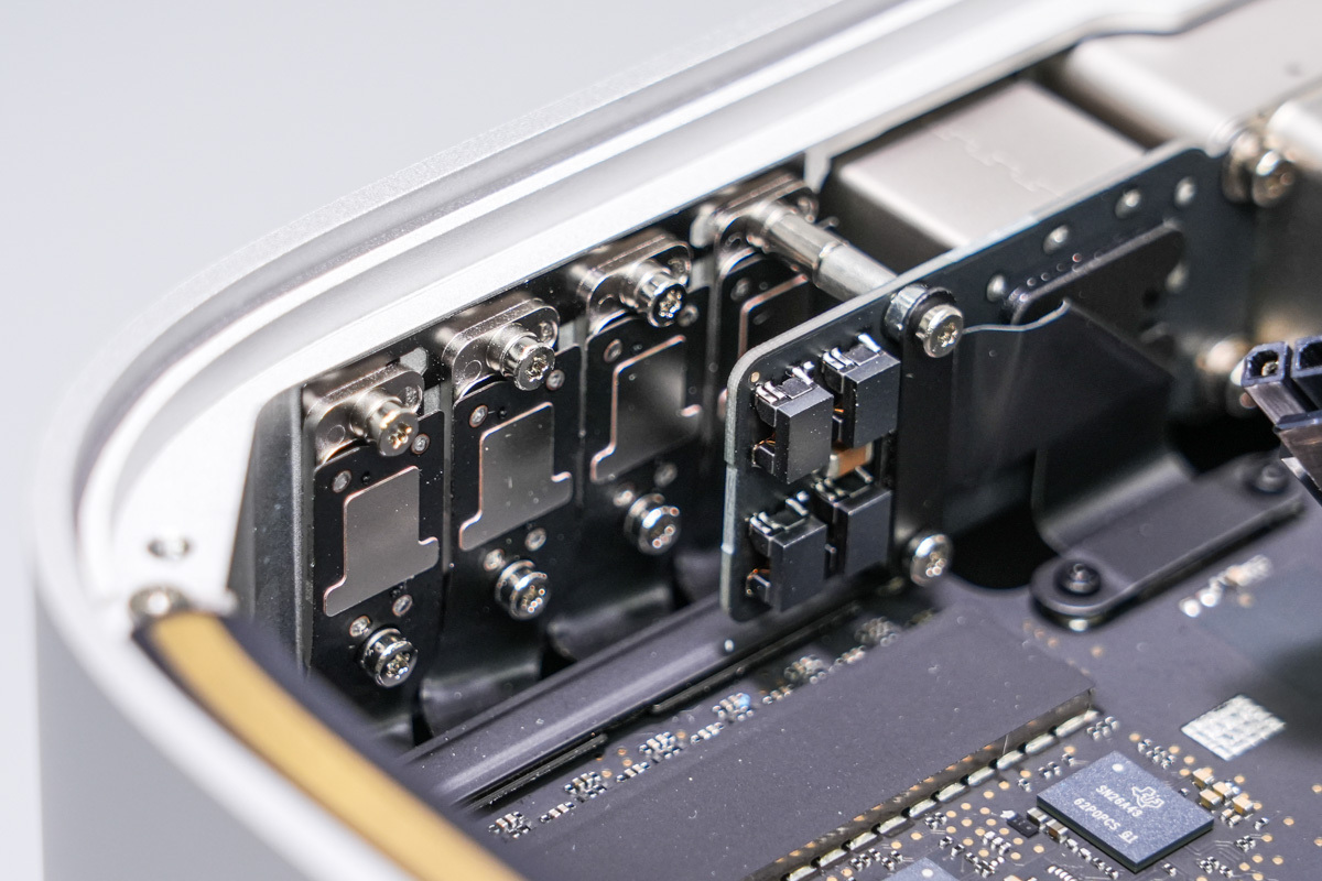
The Thunderbolt 5 ports connect to a PCB via a flexible flat cable.
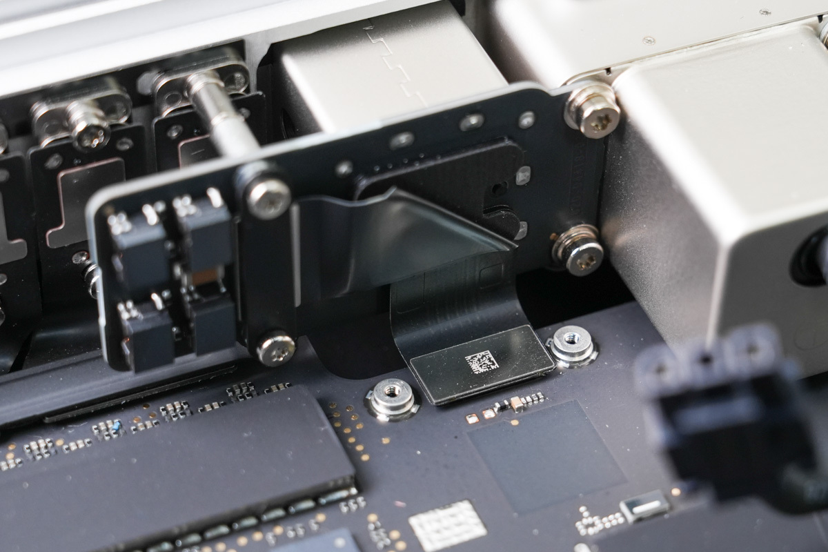
The 10Gb Ethernet port is soldered to a separate PCB, secured with screws, and connected via a flexible flat cable.
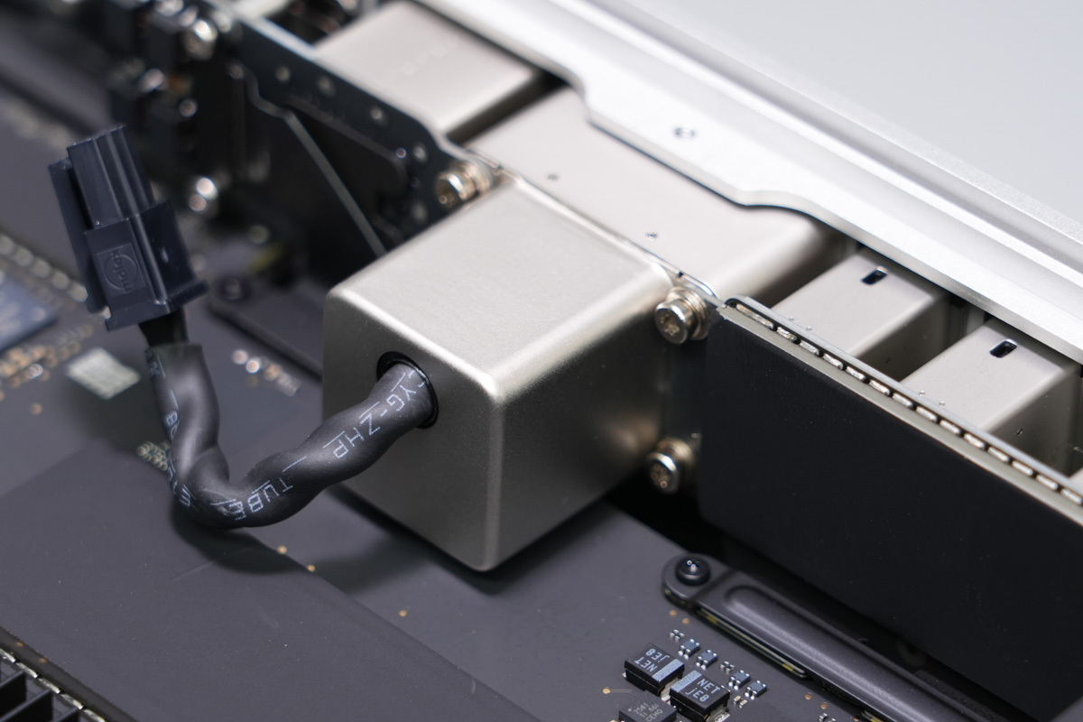
The AC power input features a filter secured with screws.
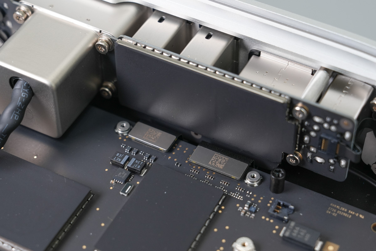
The USB-A ports, HDMI port, and 3.5mm audio jack are soldered to a separate PCB, with a shielding cover installed on the back, which connects via a flexible flat cable.
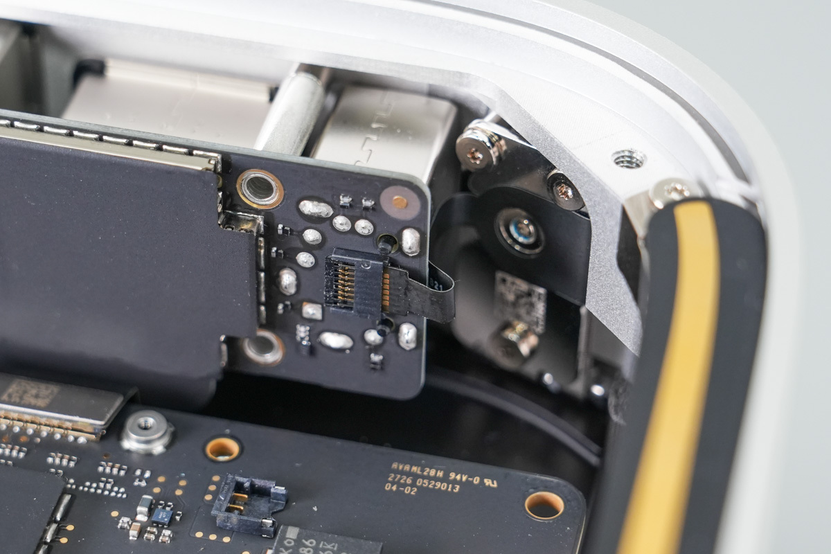
The power button connects to the PCB via a flexible flat cable.
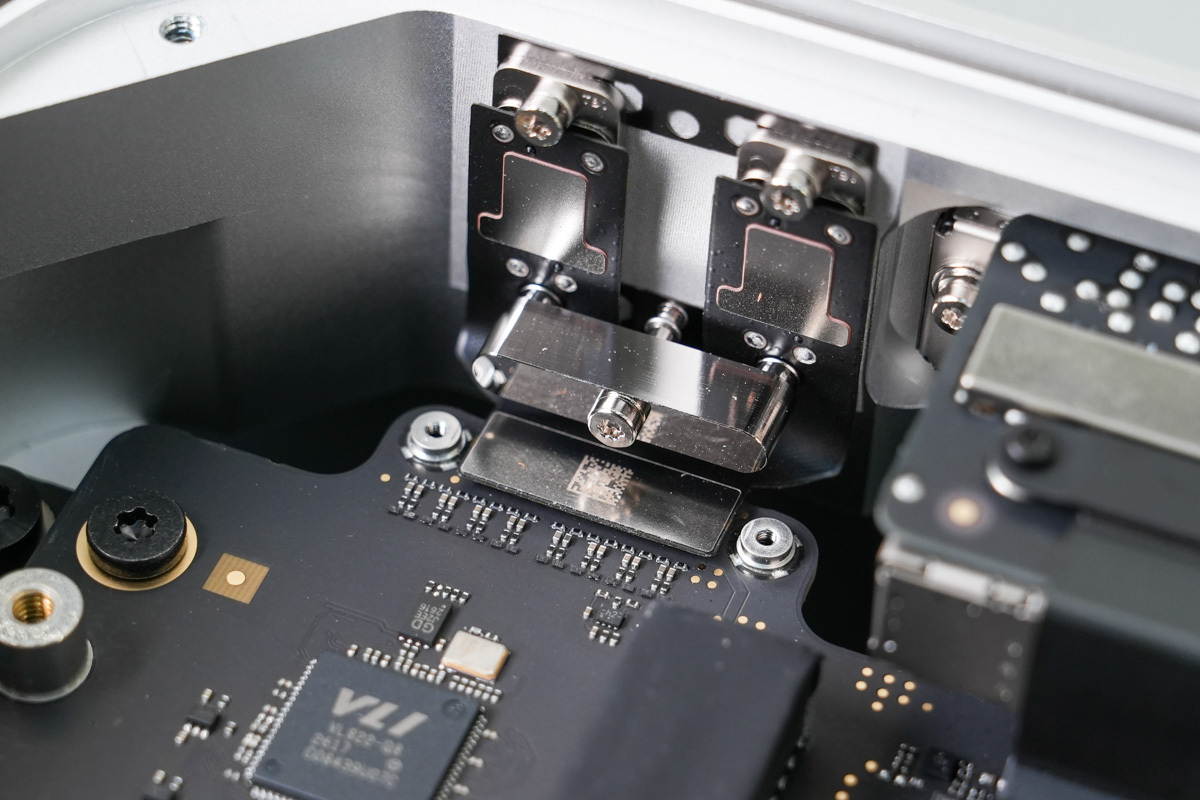
The front USB-C ports connect via a flexible flat cable.
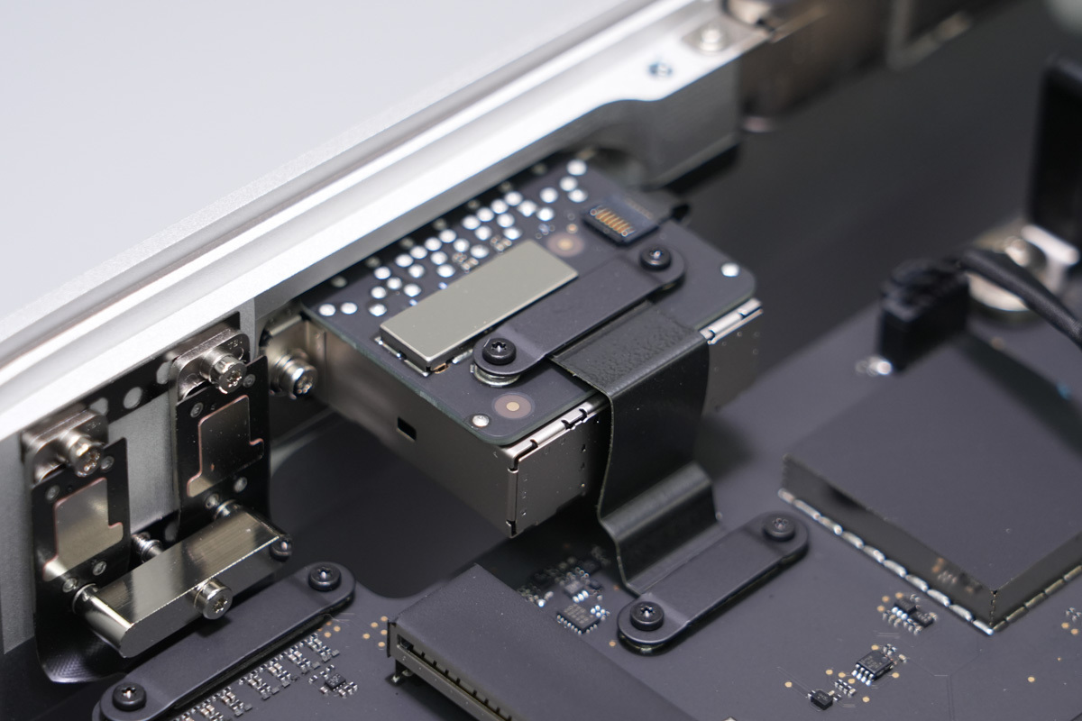
The card reader is secured with screws and connected via a flexible flat cable.
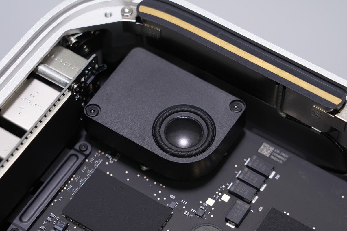
The speaker is secured to the mainboard with screws.
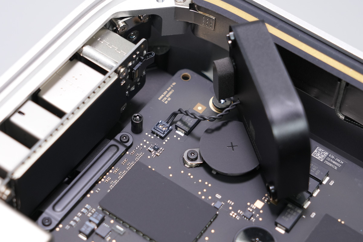
Remove the mounting screws and take out the speaker enclosure.
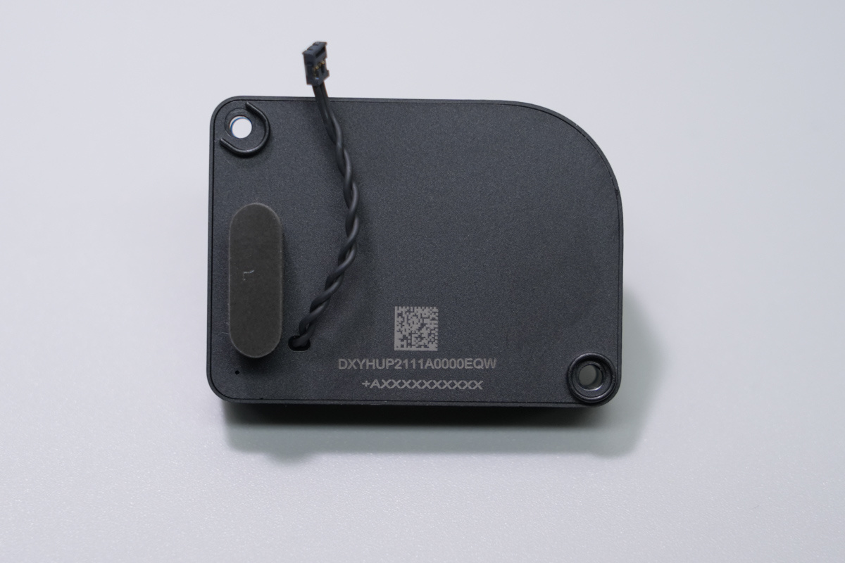
A connecting cable is located on the back of the speaker enclosure.
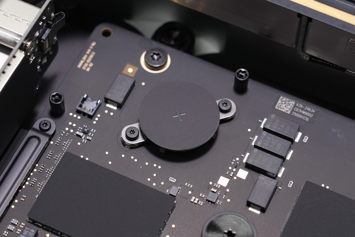
The RTC battery is secured with a metal retaining bracket.
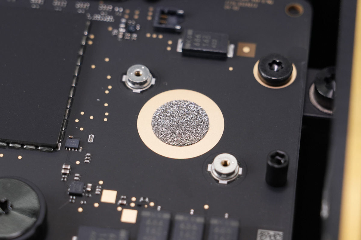
Conductive foam is attached at the corresponding negative battery contact.
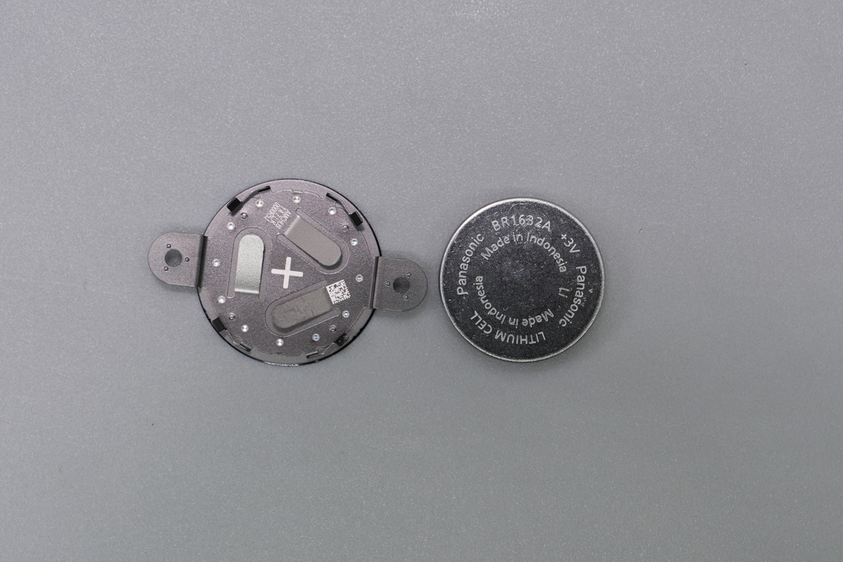
A positive polarity symbol is marked inside the battery retaining bracket.
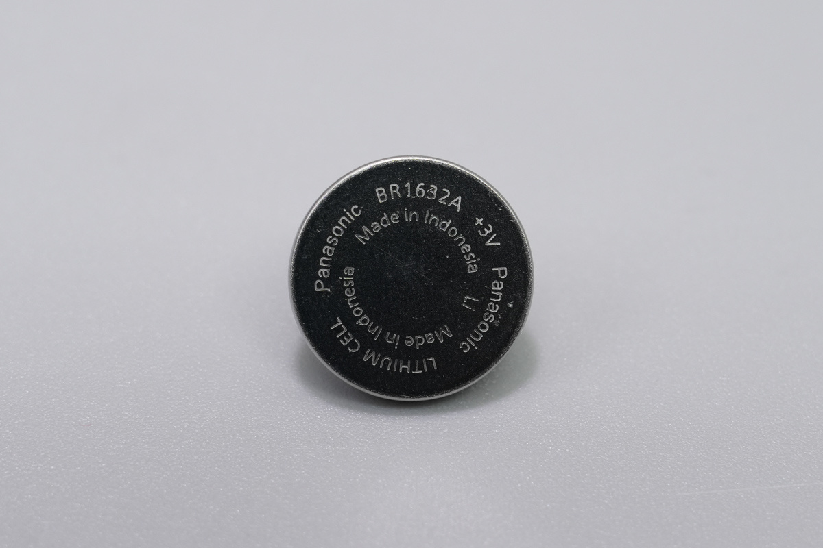
The RTC battery is from Panasonic, model BR1632A, belonging to the high-temperature-resistant BR series of lithium carbon monofluoride batteries. It is rated at 3V and 120mAh, with an operating temperature range of -40°C to 125°C.
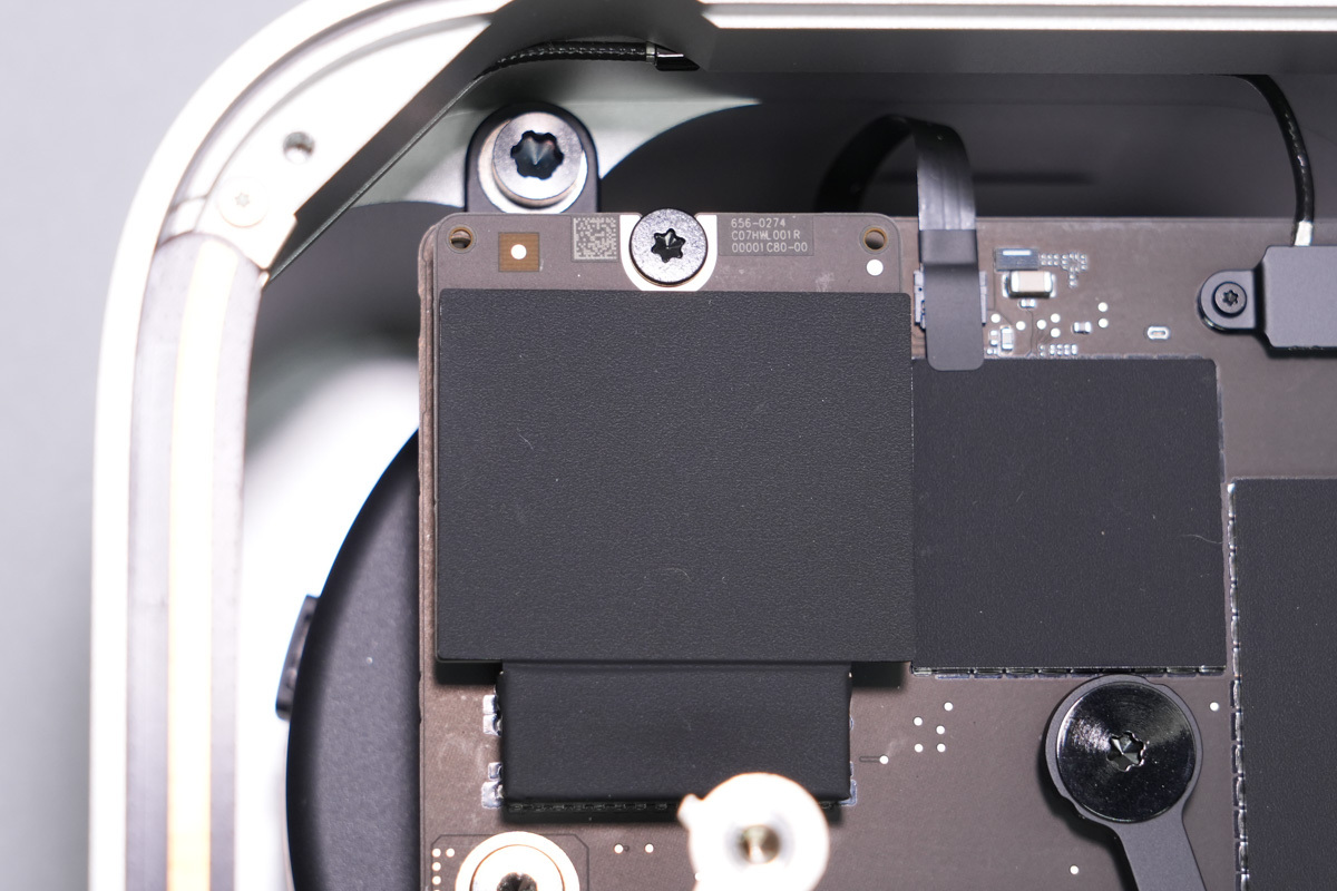
The solid-state drive uses a PCB design, is secured with screws, and is covered with a graphite thermal pad sticker.
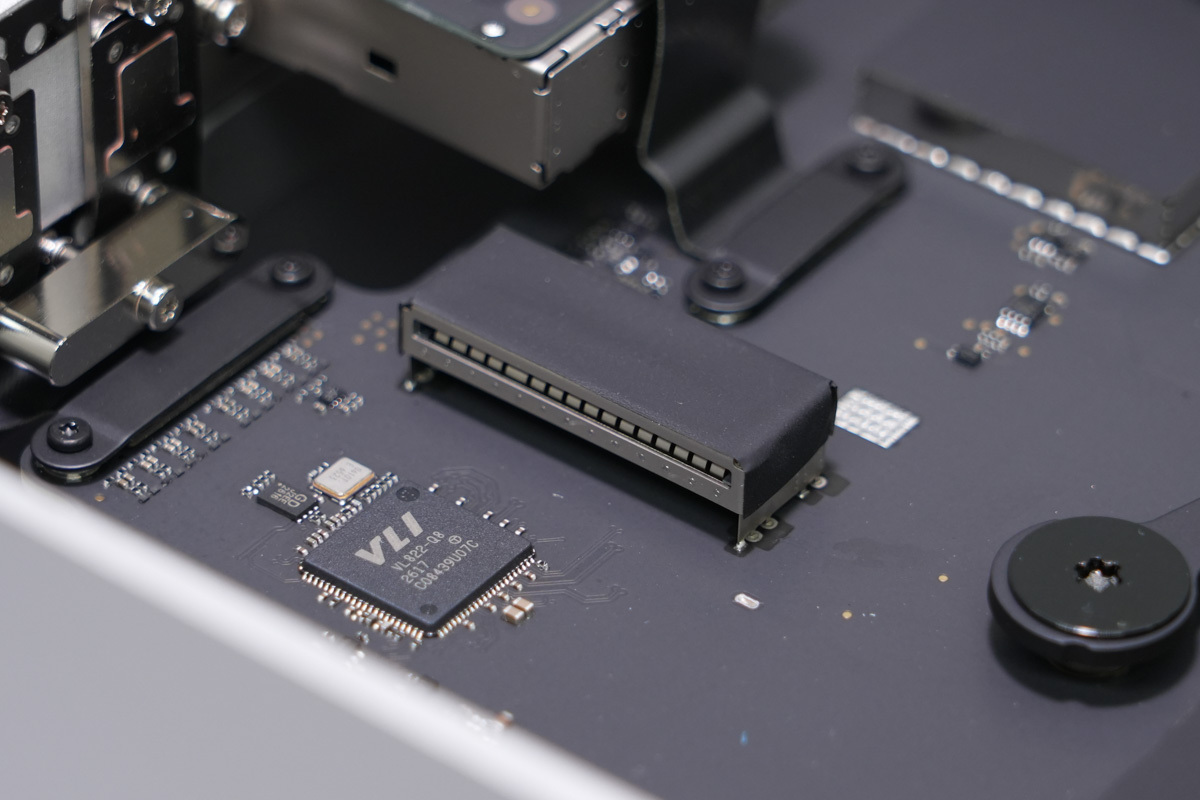
A reserved space for an additional solid-state drive is provided on the opposite side.
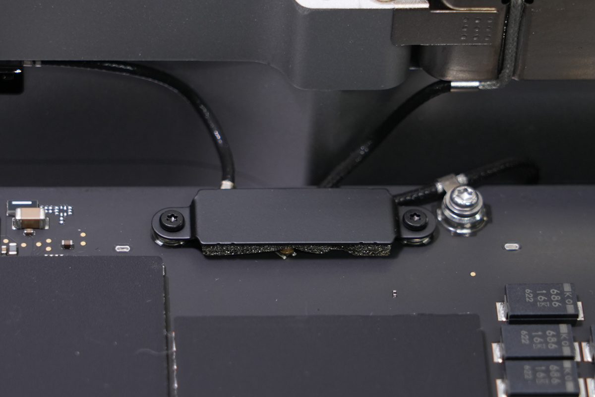
The Wi-Fi antenna connector is secured with a cover.
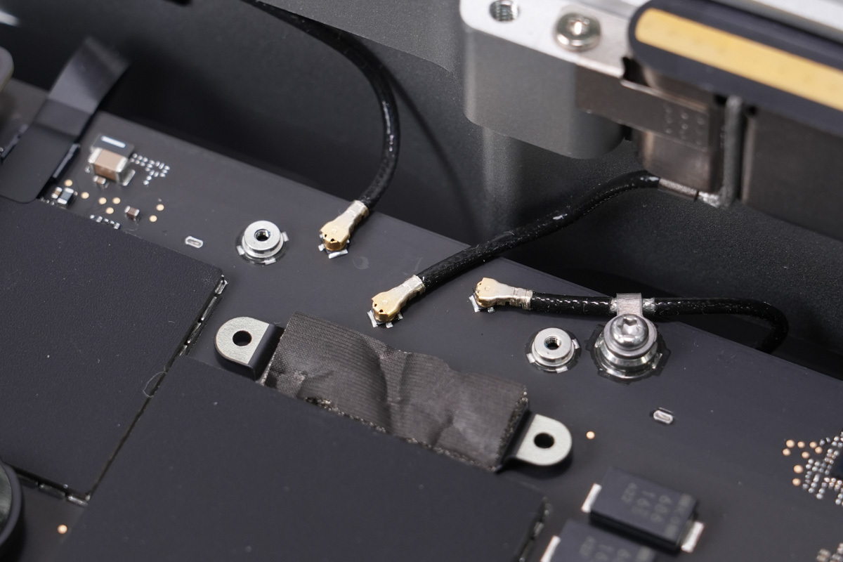
The Wi-Fi antenna connector beneath the retaining bracket.
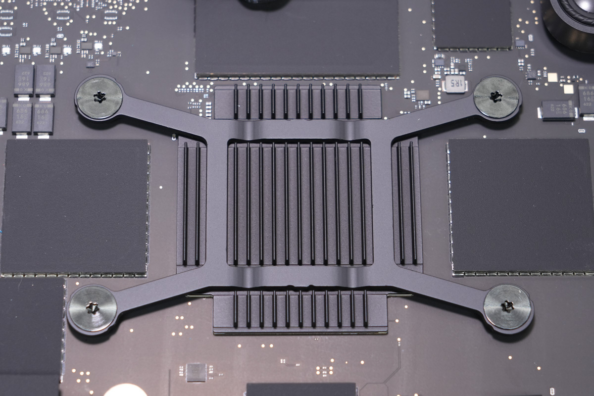
The heatsink is secured with screws and a retaining bracket.
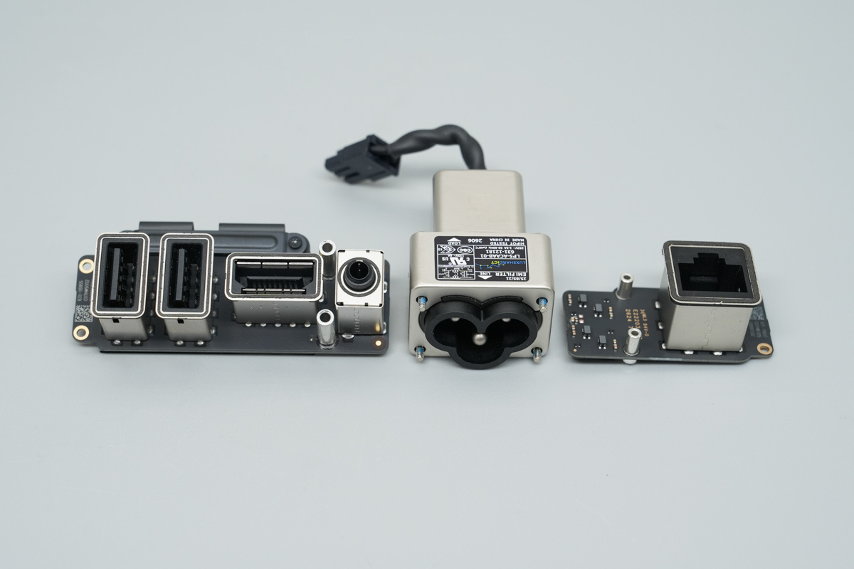
Remove the connecting PCB and AC power socket from the chassis.
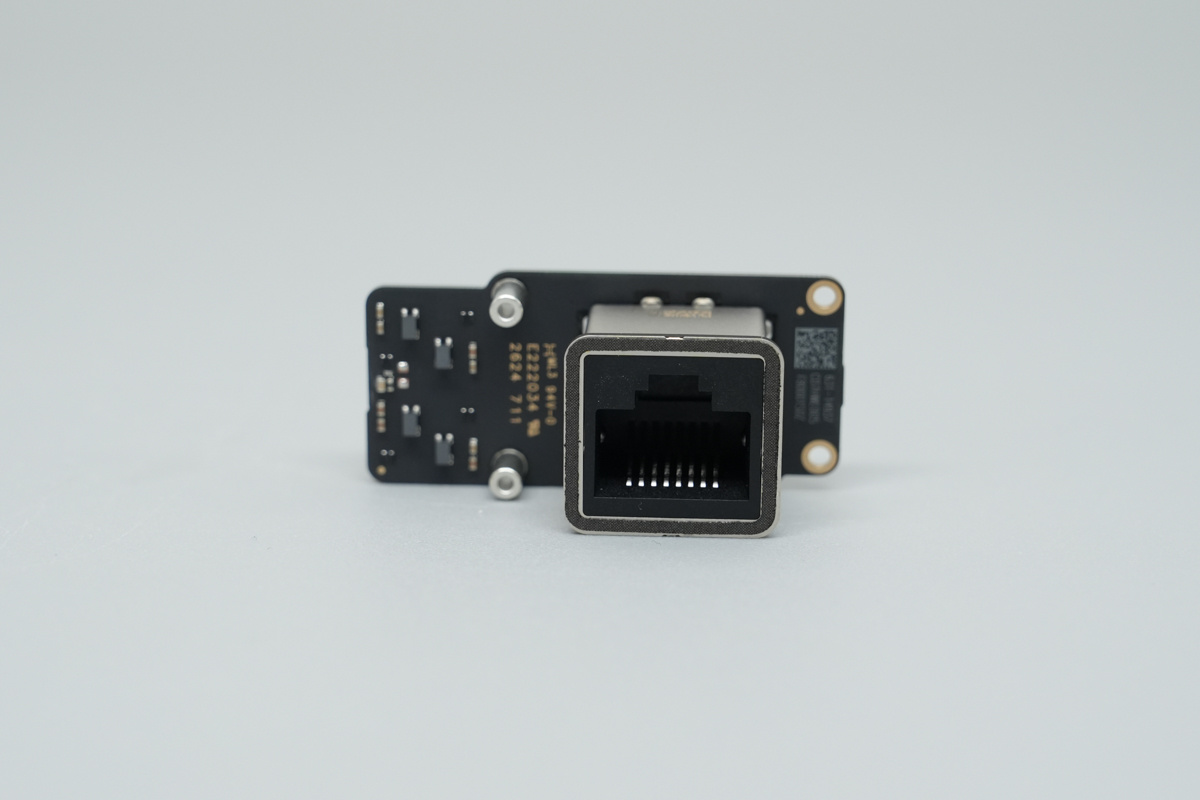
The Ethernet jack is soldered to a separate PCB.
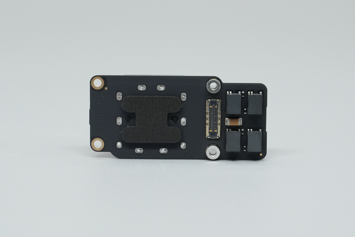
The back of the PCB features a connector and a transformer.
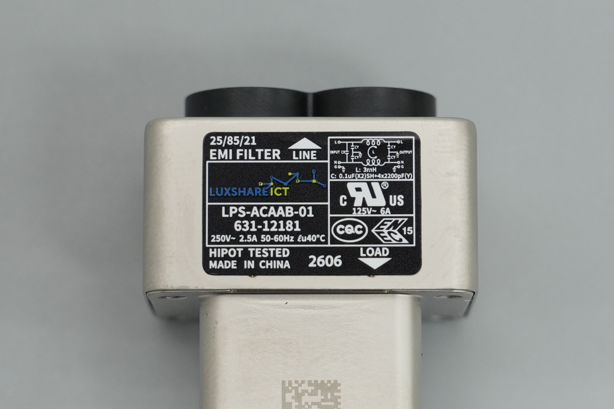
The input filter socket is from LUXSHARE-ICT.
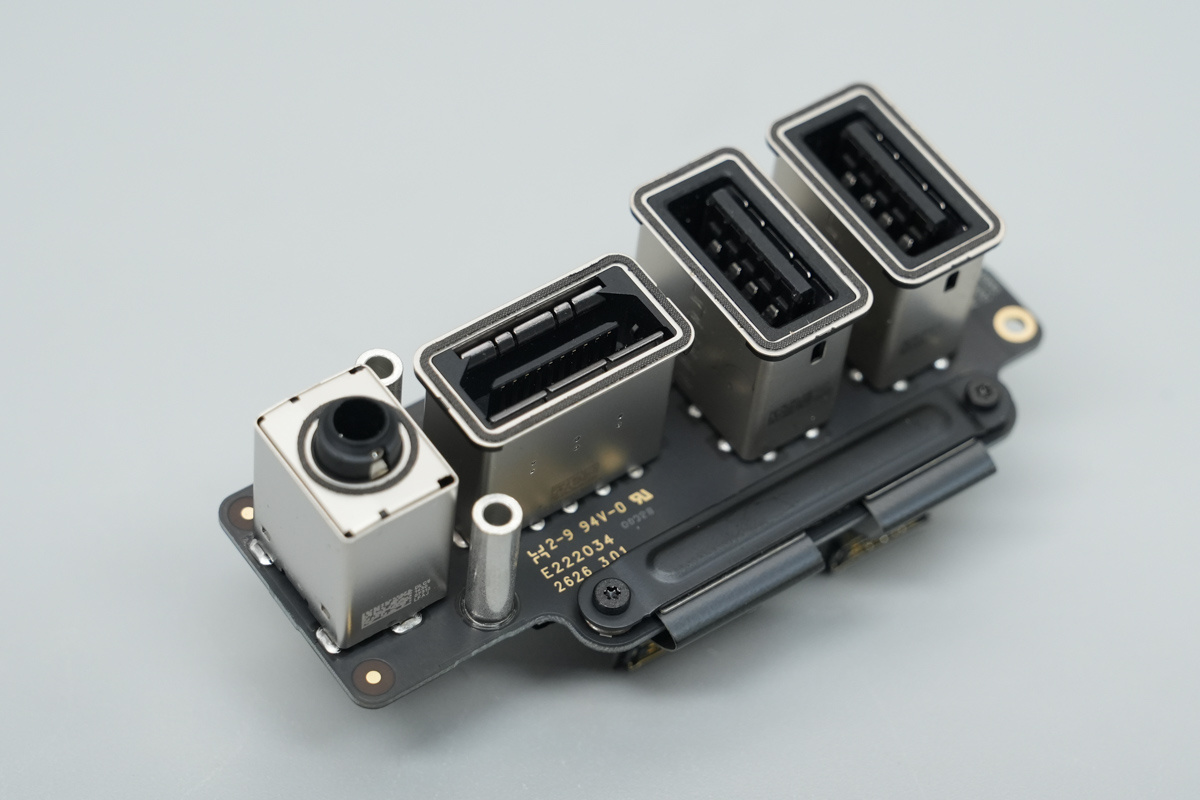
The bottom of the PCB features a connector secured with a retaining plate and screws.
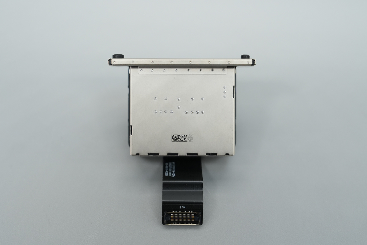
The card reader features a metal shielding enclosure.
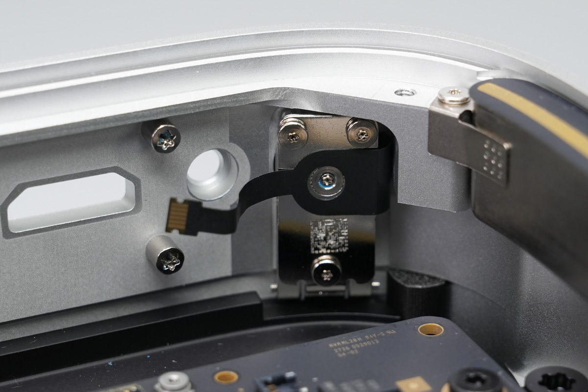
The power switch is secured inside the chassis with screws.
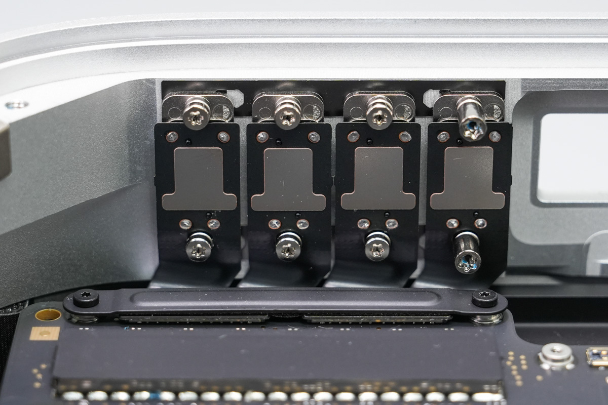
The Thunderbolt 5 ports are secured inside the chassis with screws.
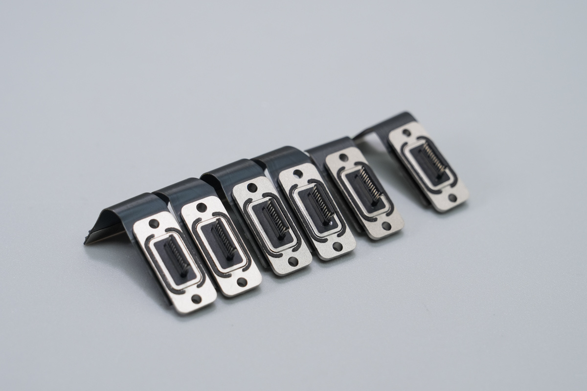
The ports are secured with screws for easier servicing and replacement.
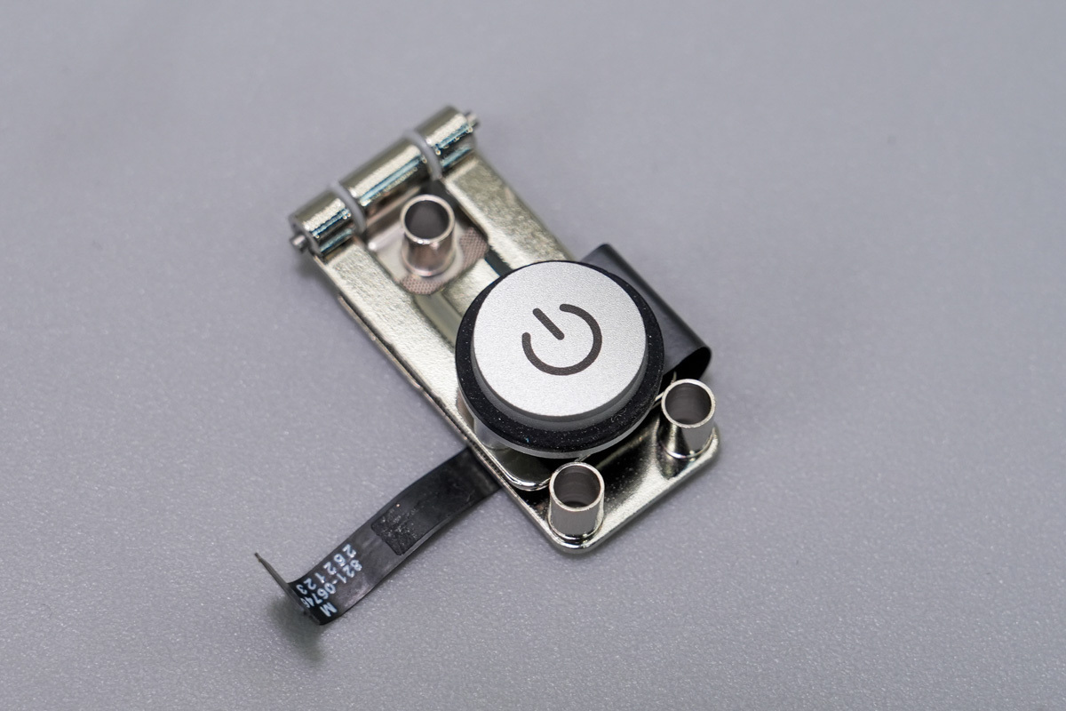
The power button assembly is secured inside the chassis with screws.
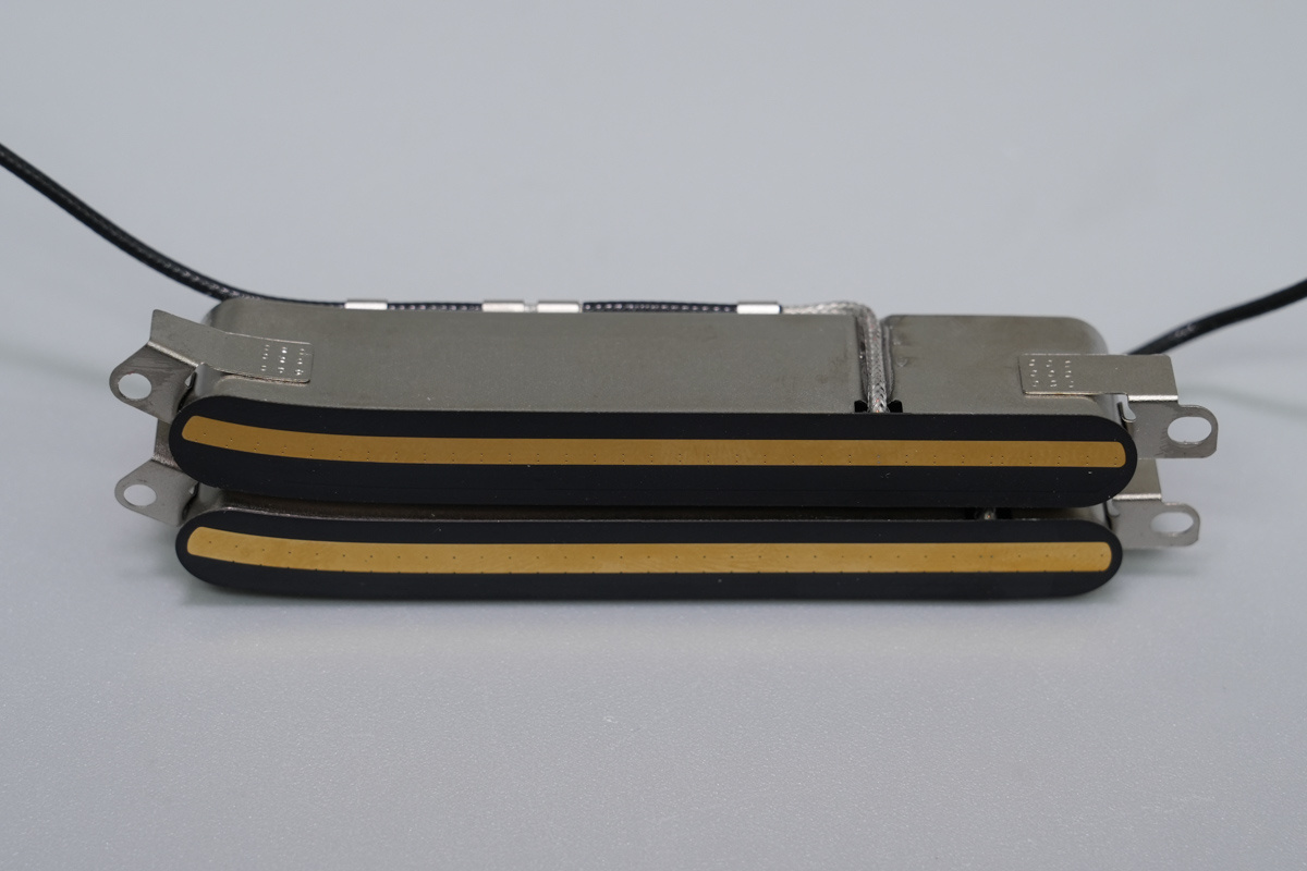
The Wi-Fi antenna is secured to the inside of the chassis with screws.
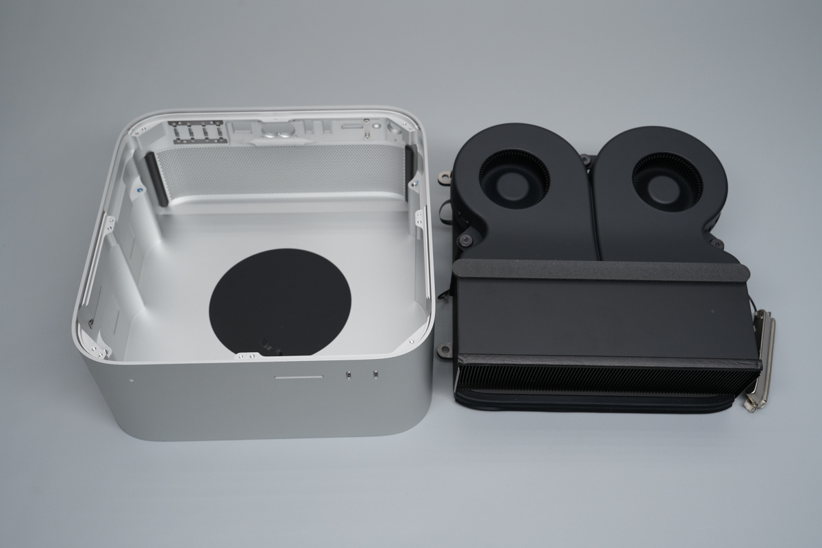
Remove the mounting screws and take out the mainboard and heatsink assembly from the chassis.
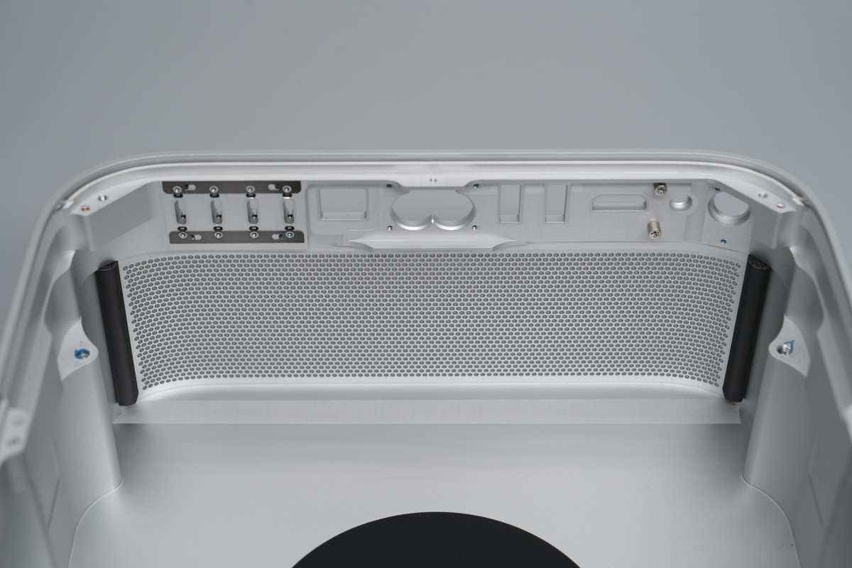
Conductive fabric is installed on both sides of the ventilation outlet for grounding and sealing.
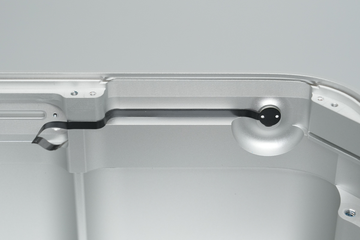
The power indicator connects via a flexible flat cable.
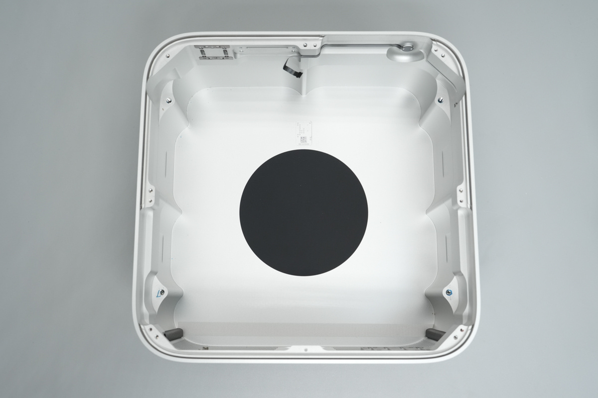
The chassis interior, which is CNC-machined from a single piece of aluminum alloy, with a black sticker applied in the center.
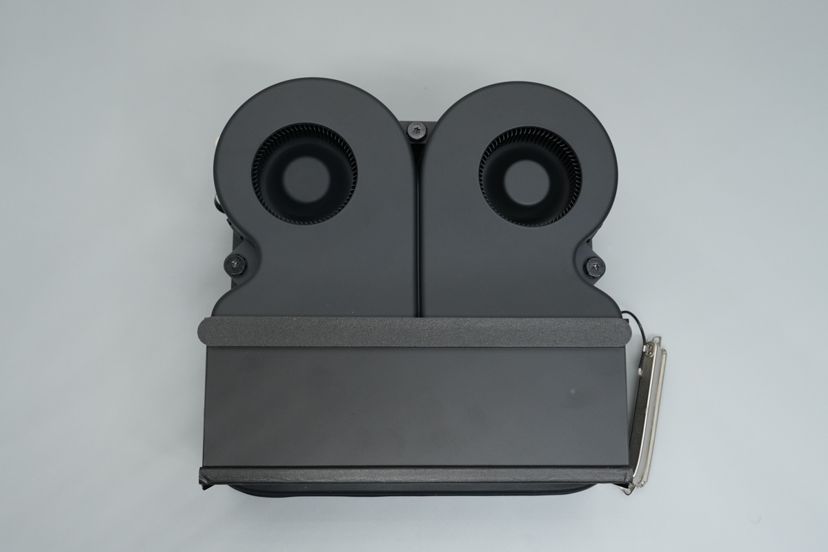
The mainboard is covered by the cooling fan and heatsink assembly.
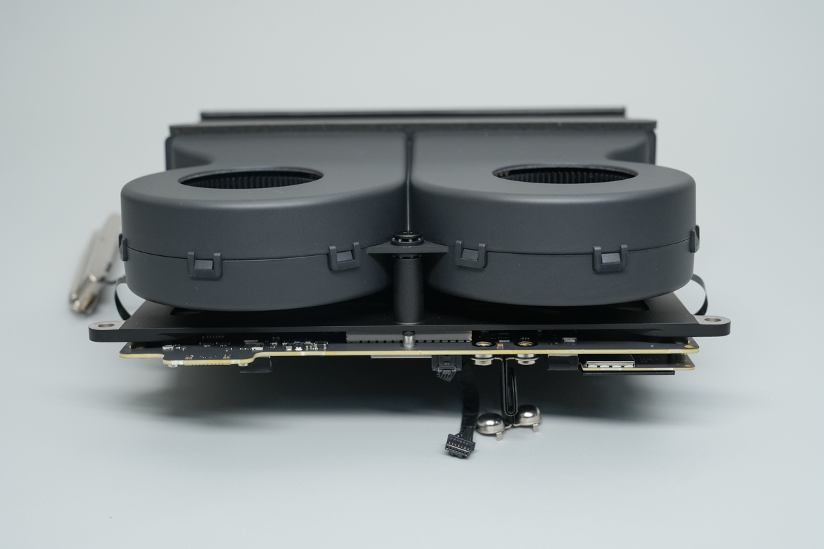
The cooling fan is secured to the heatsink assembly with screws.
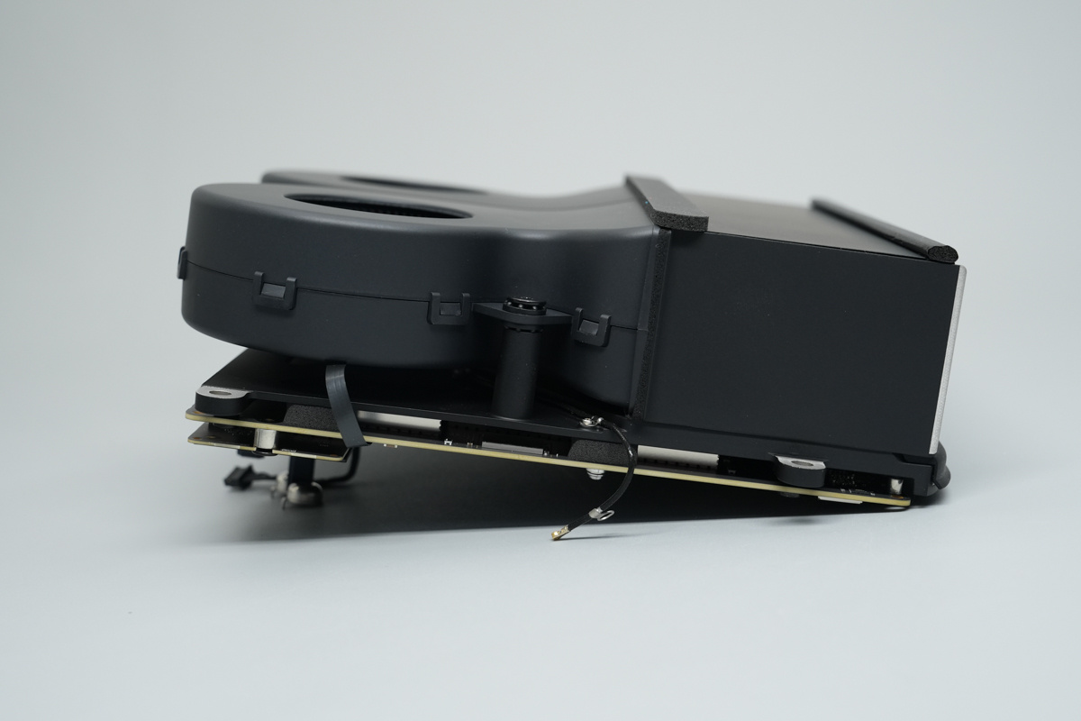
Additional mounting screws are provided on the side.
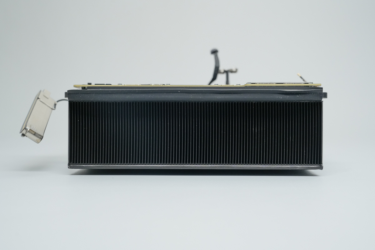
The large heatsink fins.
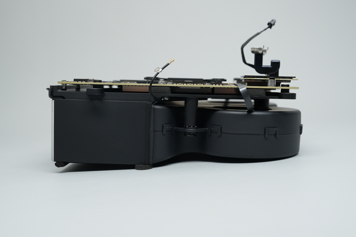
The side of the heatsink assembly, cooling fan, and mainboard.
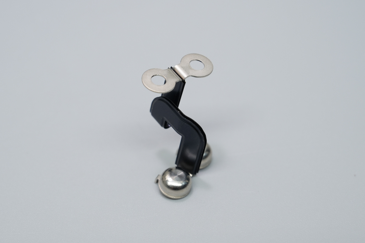
Remove the screws securing the connecting flexible flat cable.
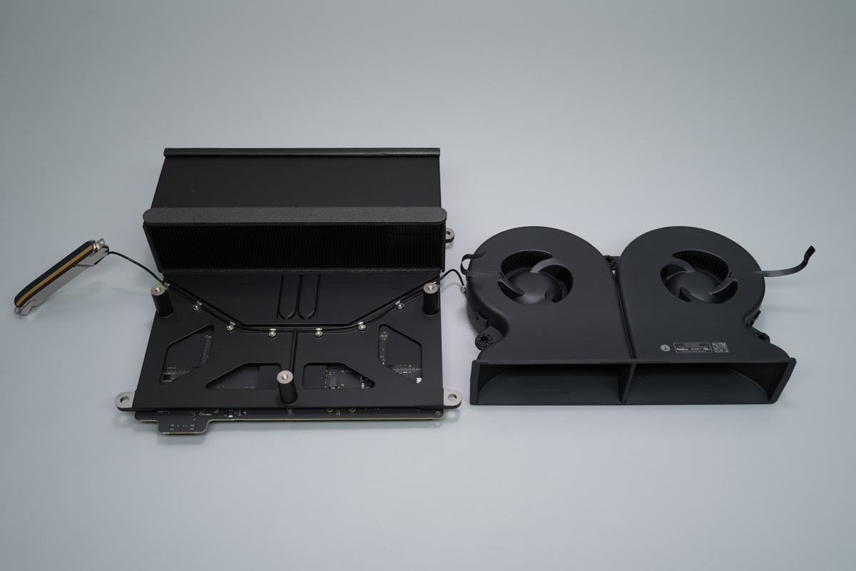
Remove the mounting screws and take off the cooling fan.
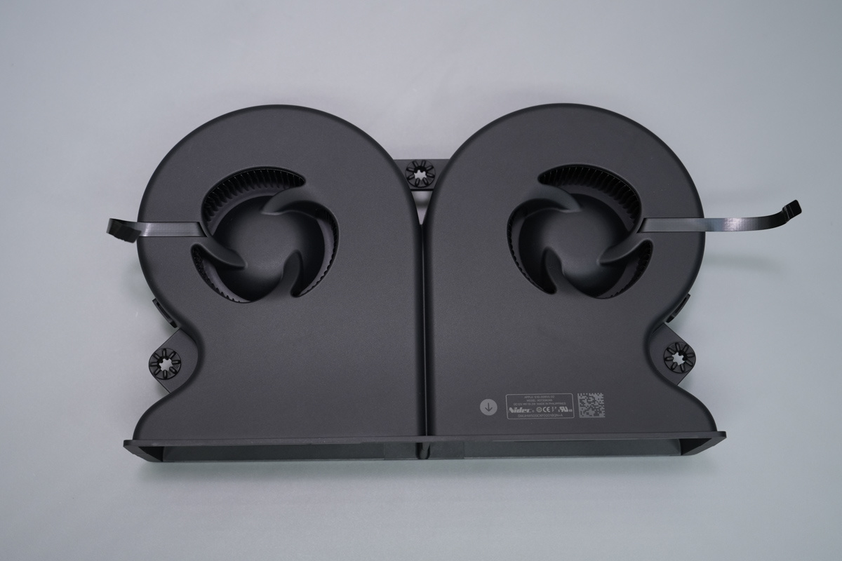
The cooling fan features an integrated design.
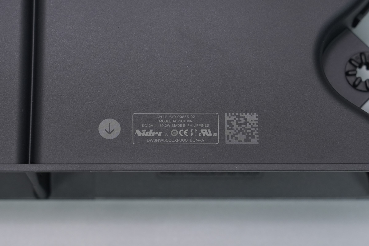
The cooling fan is from Nidec, model AD720K04A, rated at 12V 19.2W.
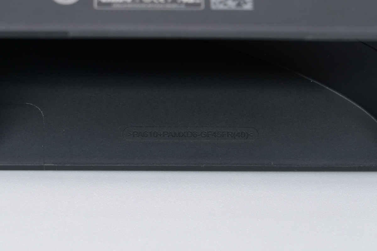
The inside of the air outlet is marked with the chassis material spec: >PA610+PAMXD6-GF45FR(40)<.
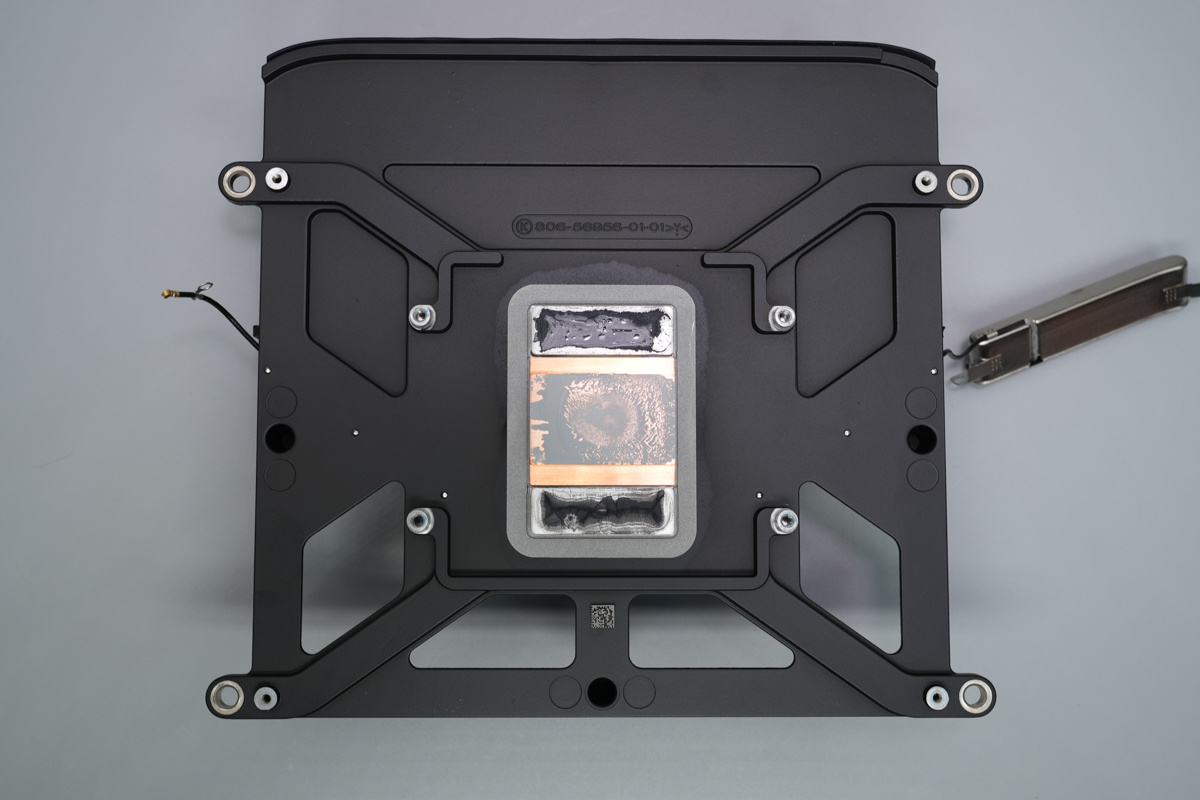
Remove the mounting screws to separate the mainboard from the heatsink assembly.
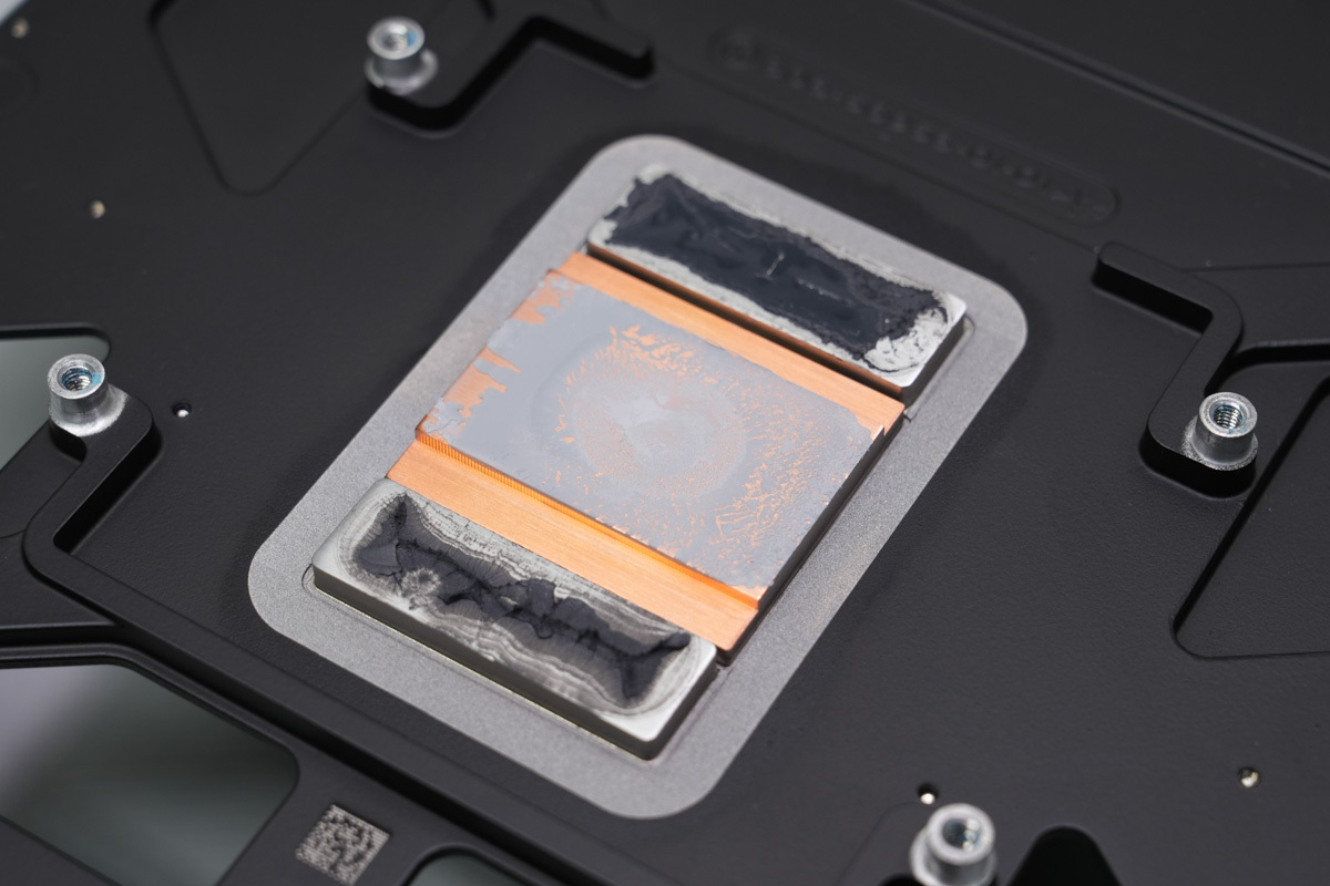
The heatsink assembly features a copper base corresponding to the processor, with thermal gel applied on both sides.
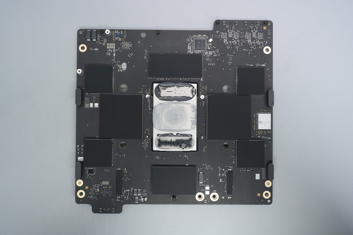
The M5 Max chip is located in the center of the mainboard, with shielding cans arranged around the surrounding area.
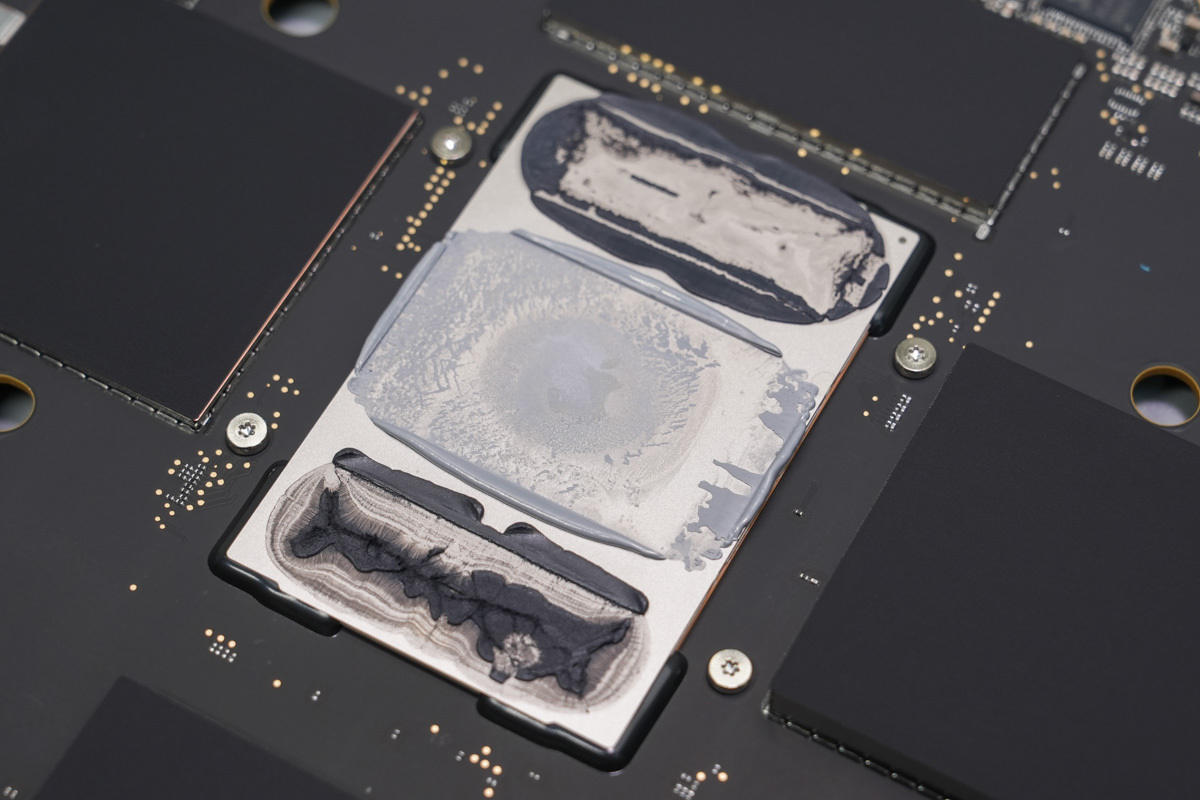
The M5 Max chip features a metal heat spreader. Thermal grease is applied in the center, while thermal gel is applied along the upper and lower edges.
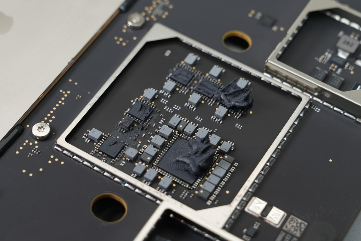
Thermal gel is applied to the chips inside the shielding cans.
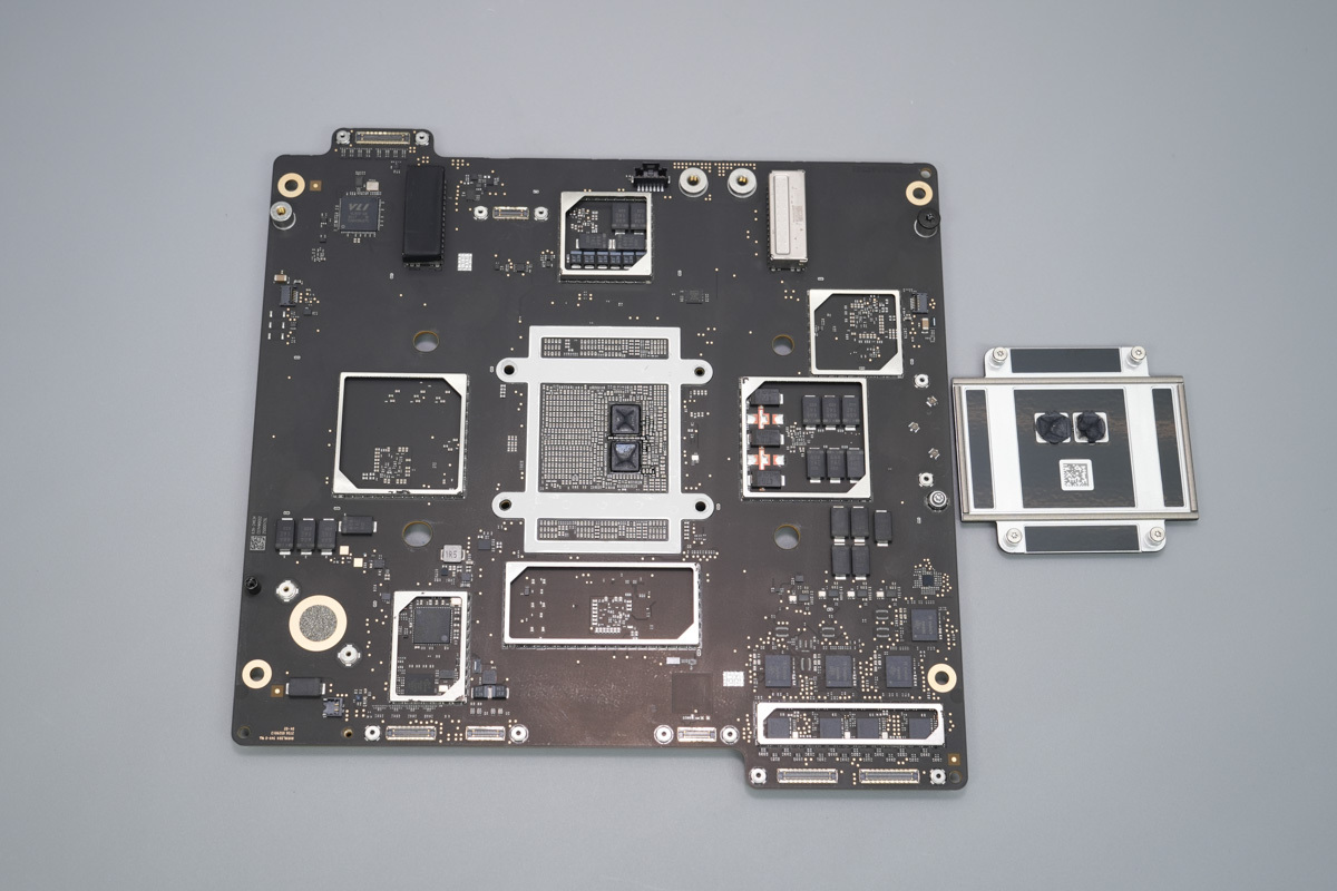
Remove the retaining plate on the back of the M5 Max chip.
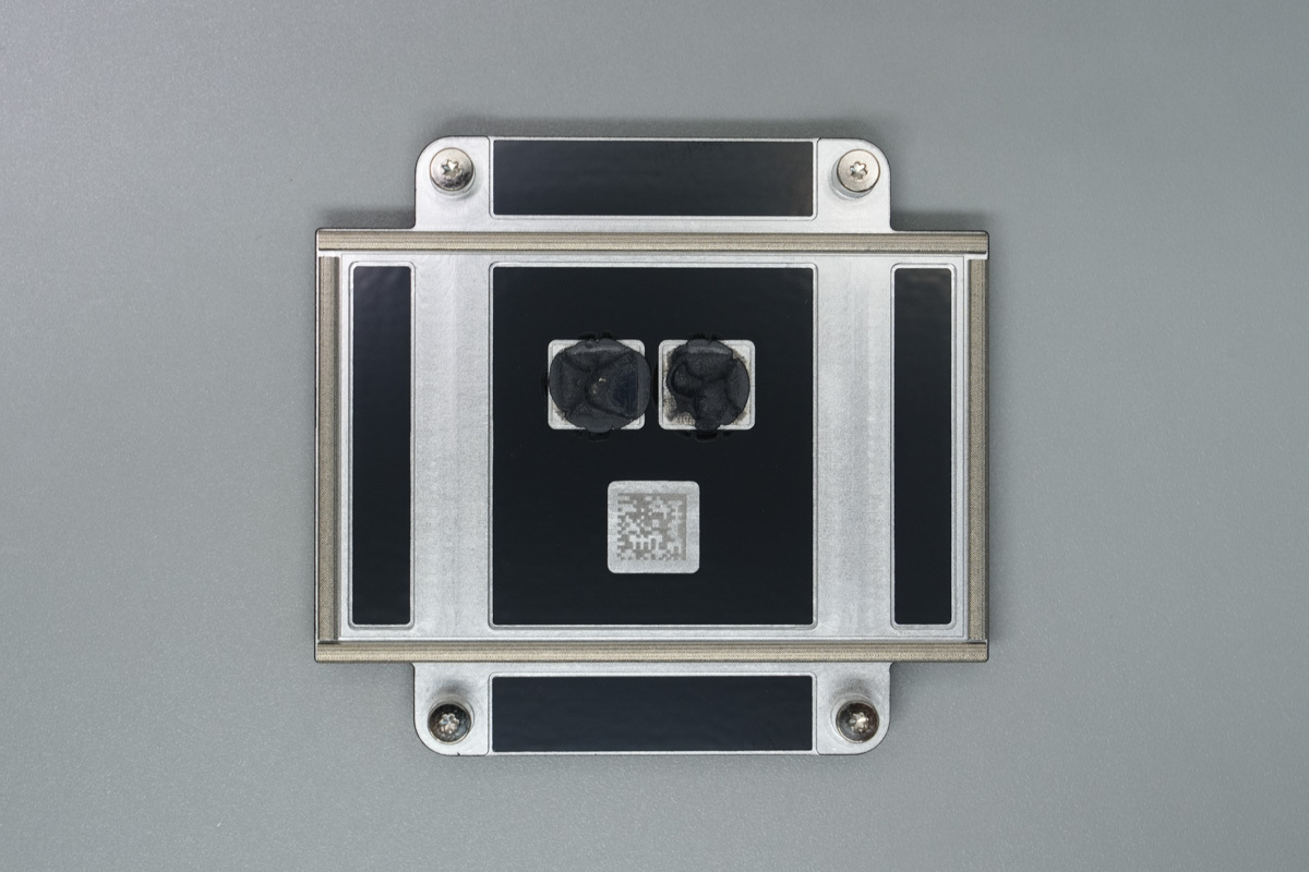
Thermal gel is applied inside the retaining plate to facilitate heat transfer from the chip.
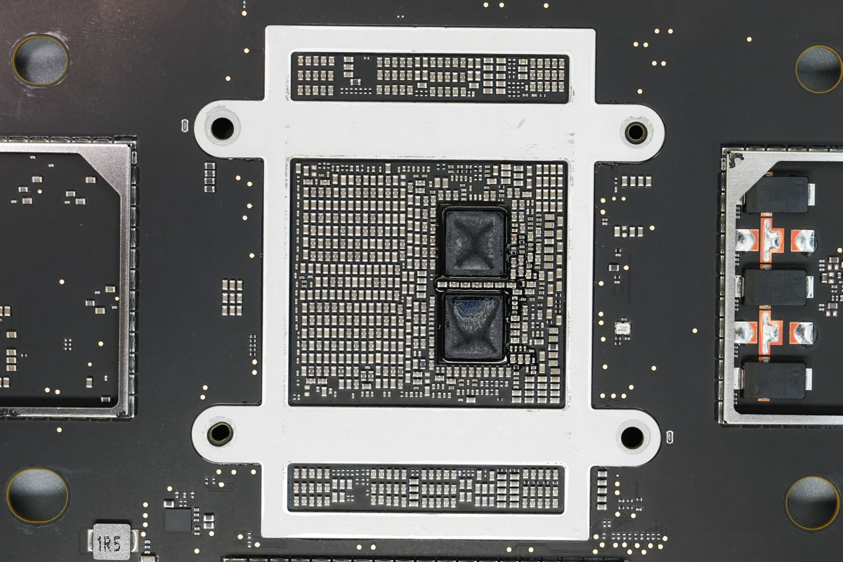
Metal shims are attached to the back of the PCB to cushion and distribute pressure.
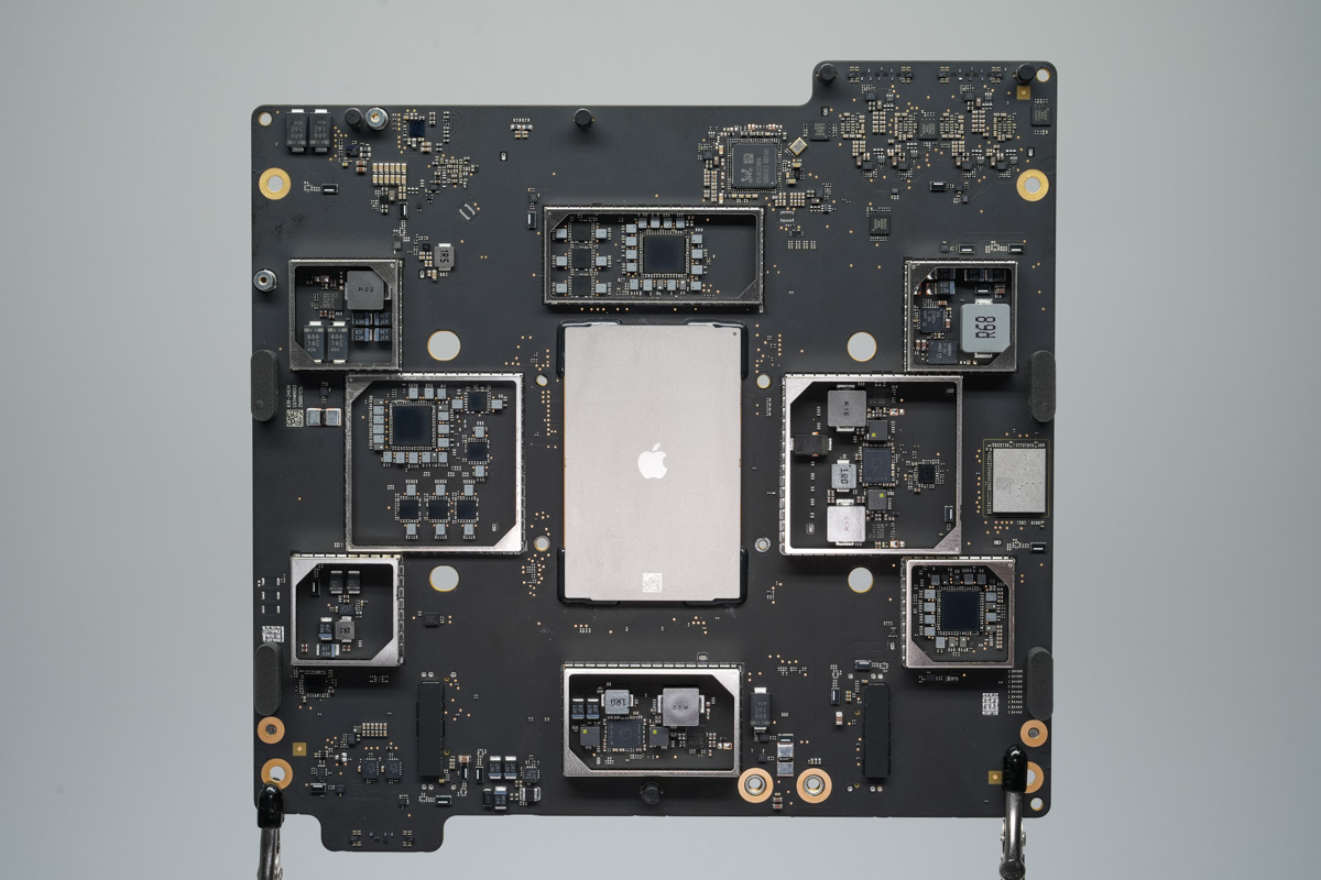
The M5 Max chip is located in the center of the PCBA module. The shielding cans contain PMICs and power inductors. Filter capacitors are located in the upper-left corner, a USB-C power switch is located in the lower-left corner, and a network controller chip and memory are located in the upper-right section.
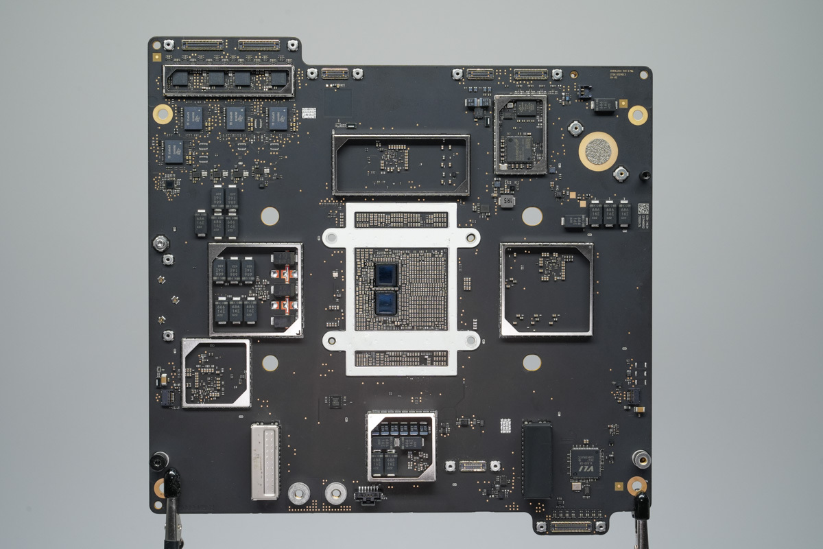
The back of the PCBA module also features shielding cans. The cans on the left and bottom contain filter caps, while the upper-left can houses a Thunderbolt controller. A USB-C controller is located beneath the shielding can. SSD slots are provided on both sides of the bottom section. The shielding can on the right contains a USB conversion chip and an HDMI conversion chip, with a USB hub controller located below.
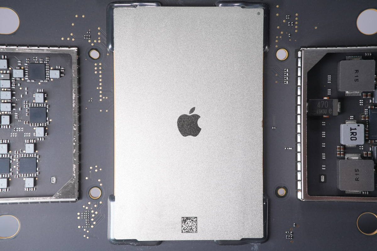
The M5 Max chip is covered by a metal heat spreader, beneath which are the SoC and memory chips.
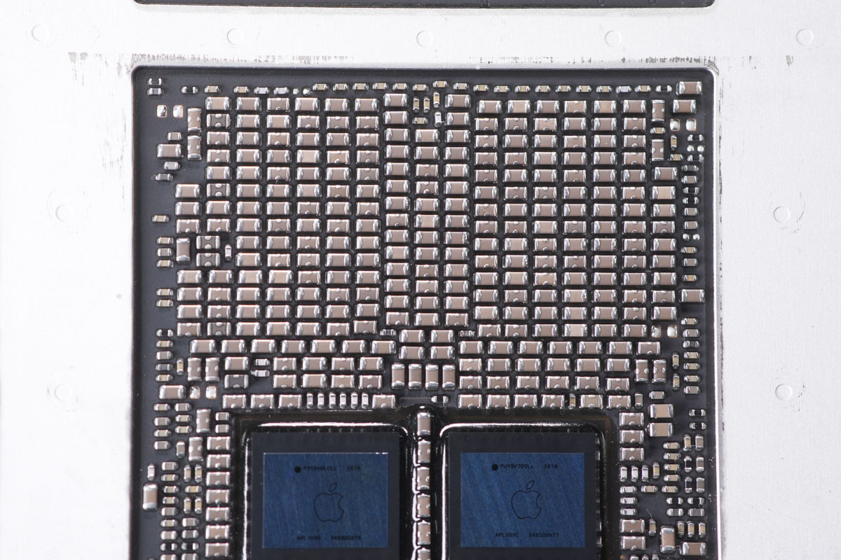
The back of the M5 Max chip features filter capacitors and PMICs.
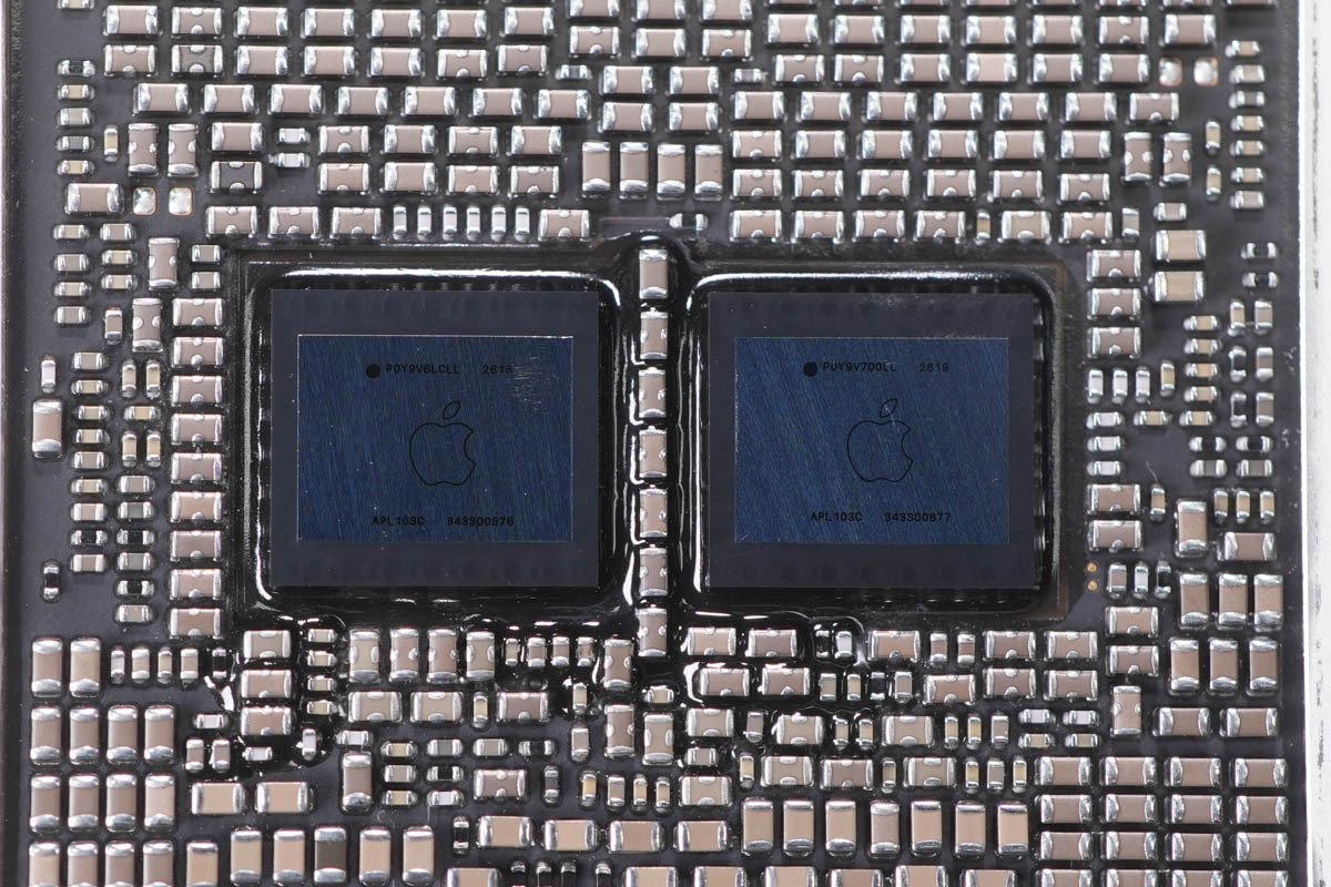
Thermal gel is applied to two PMICs for heat dissipation. Their markings are 343S00876 and 343S00877.
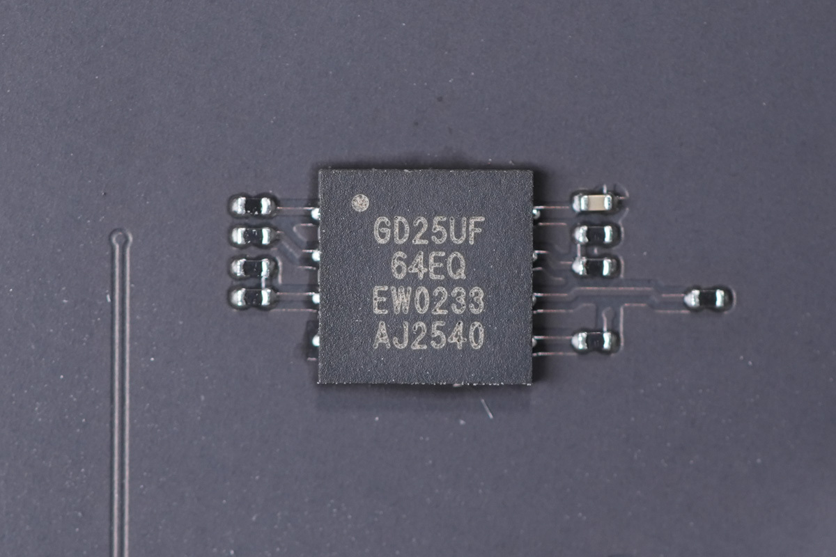
The memory chip is from GigaDevice, model GD25UF64E, with a capacity of 8MB. It supports an operating voltage of 1.14–1.26V and is housed in a USON-8 package.
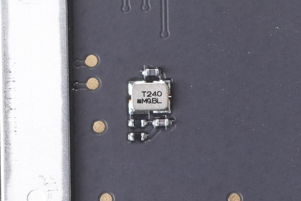
The SMD clock crystal.
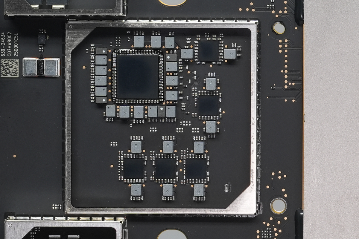
The shielding can on the left of the chip contains six PMICs and their corresponding buck inductors.
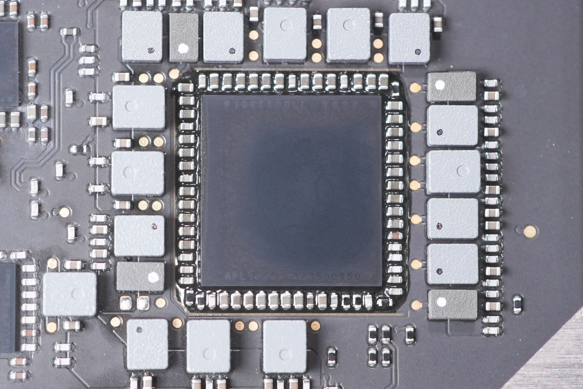
The PMIC marked 343S00960.
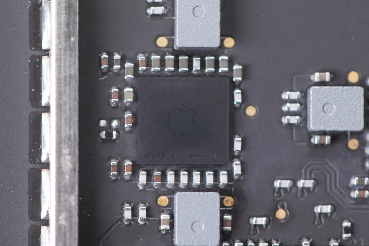
The PMIC marked 343S00892.
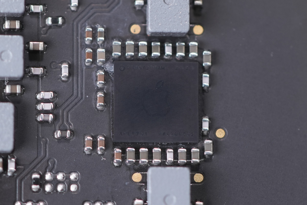
Another PMIC marked 343S00892.
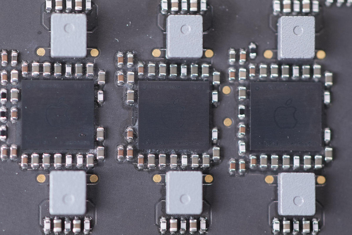
The two PMICs on the left and right are marked 343S00893, while the middle PMIC is marked 343S00892.
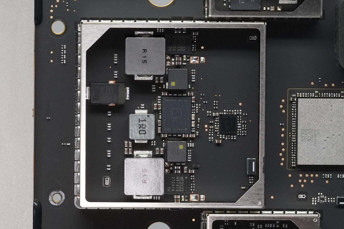
The shielding can on the right houses a PMIC, a buck inductor, filter caps, current-sense resistors, and a current-sense IC.
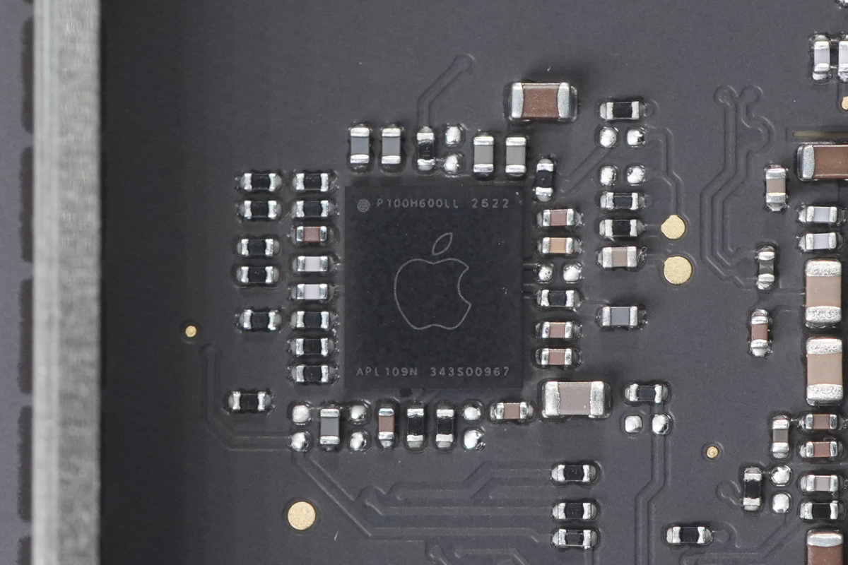
The chip marked 343S00967.
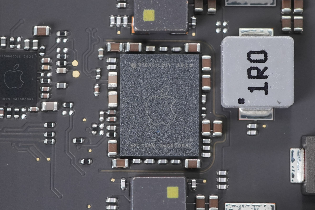
The PMIC marked 343S00966.
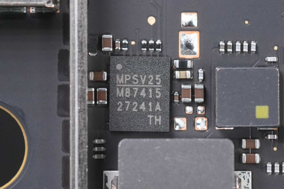
The PMIC from MPS, marked M87415.
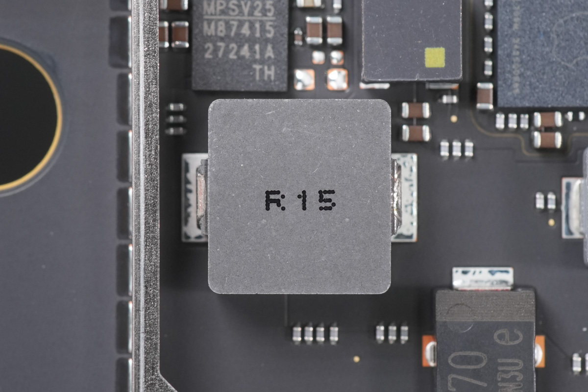
The 0.15 μH alloy inductor.
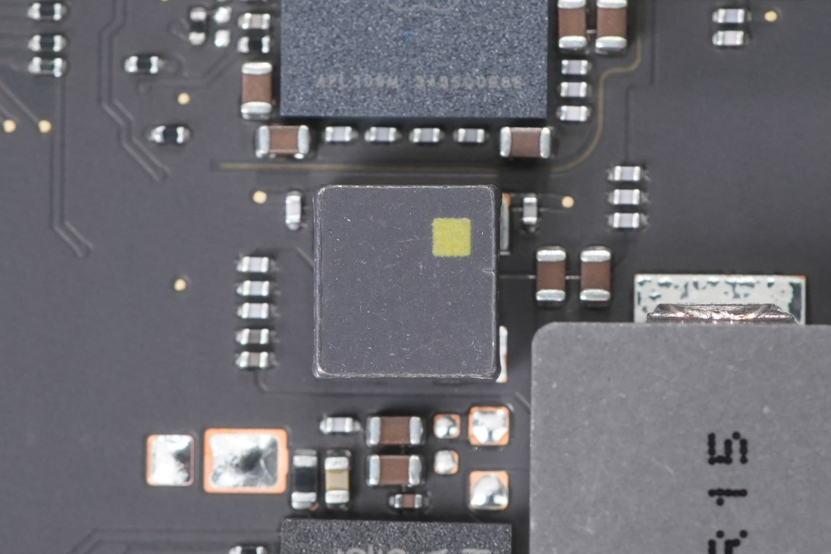
The SMD inductor.
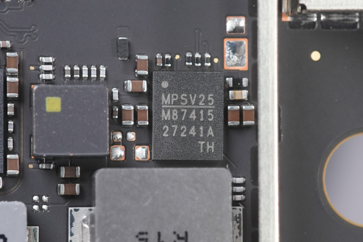
The PMIC from MPS, marked M87415.
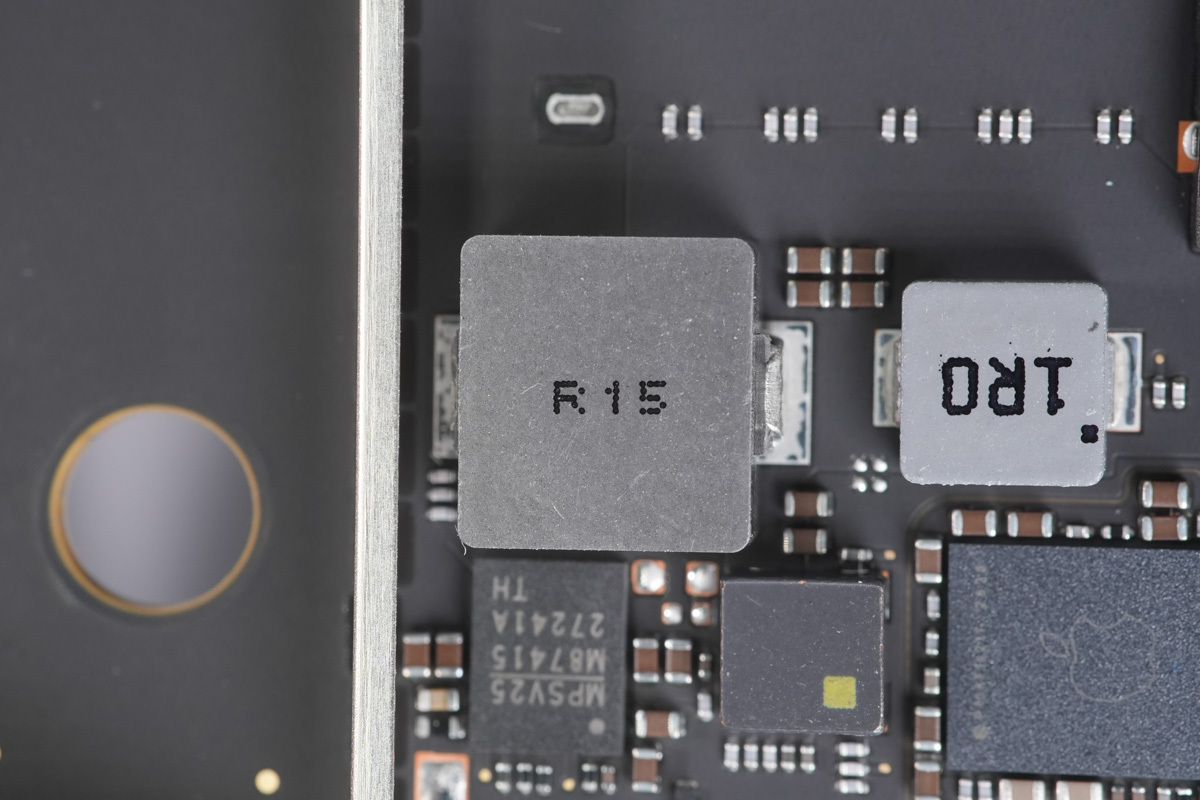
The 0.15 μH alloy inductor.
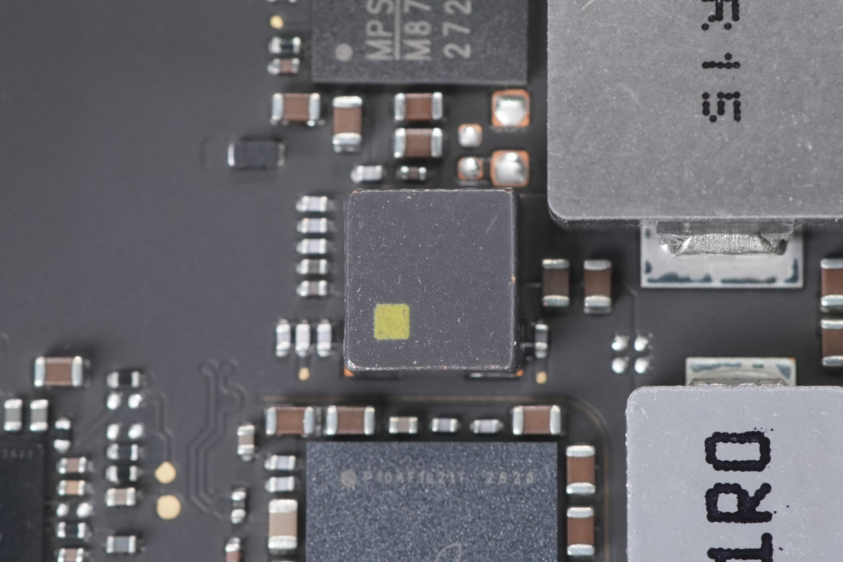
The SMD inductor.
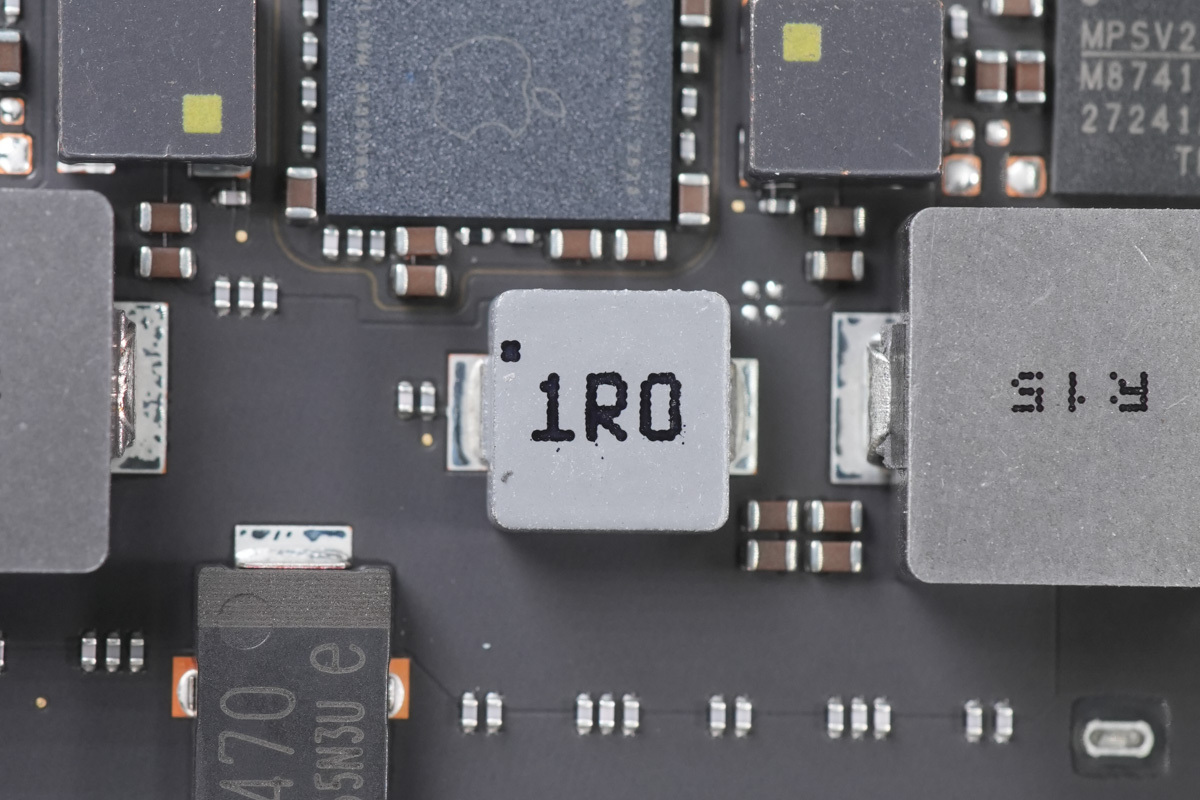
The 1 μH alloy inductor.
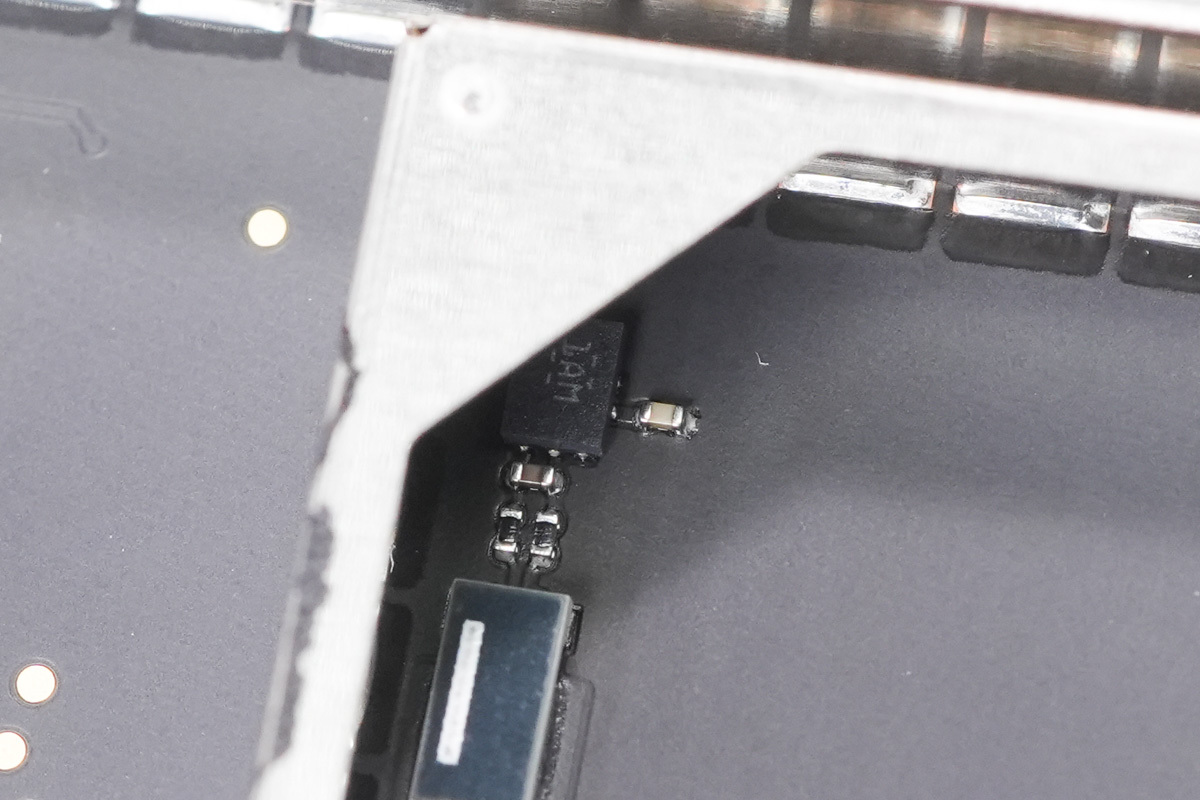
The current-sense amplifier is from TI, marked 1AM, model INA190. It is a bidirectional, low-power, zero-drift precision current-sense amplifier with a wide dynamic range. It supports a 40 V common-mode voltage and is housed in a UQFN-10 package.
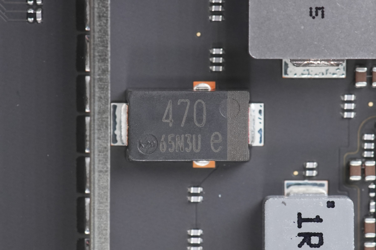
The filter cap is from Panasonic, part of the SP-CAP series of conductive polymer aluminum electrolytic caps, rated at 470 μF, 2.5 V.
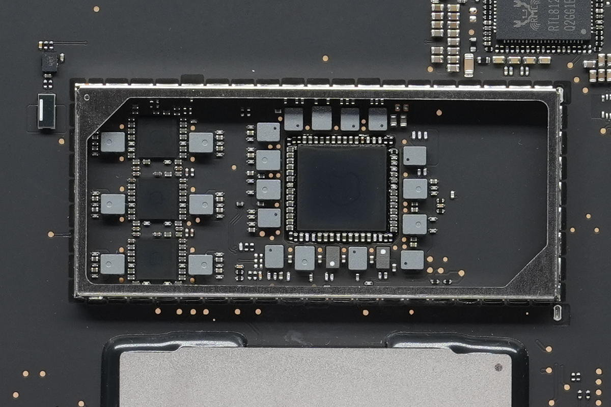
The shielding can above the chip houses four PMICs and their corresponding buck inductors.
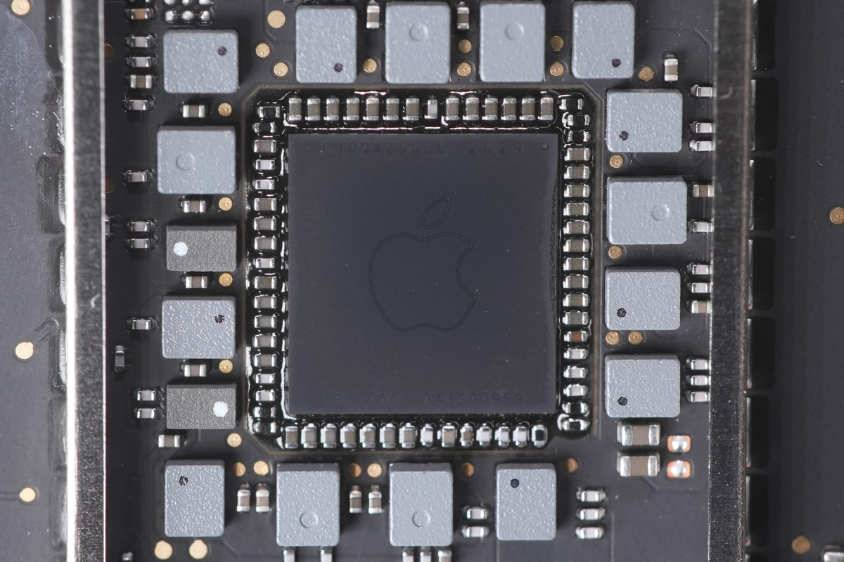
The PMIC marked 343S00959.
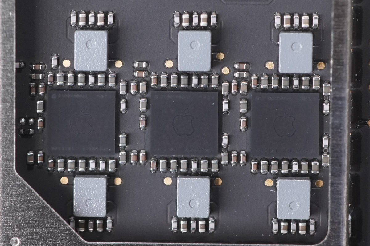
The two PMICs on the left and in the center are marked 343S00892, while the one on the right is marked 343S00893.
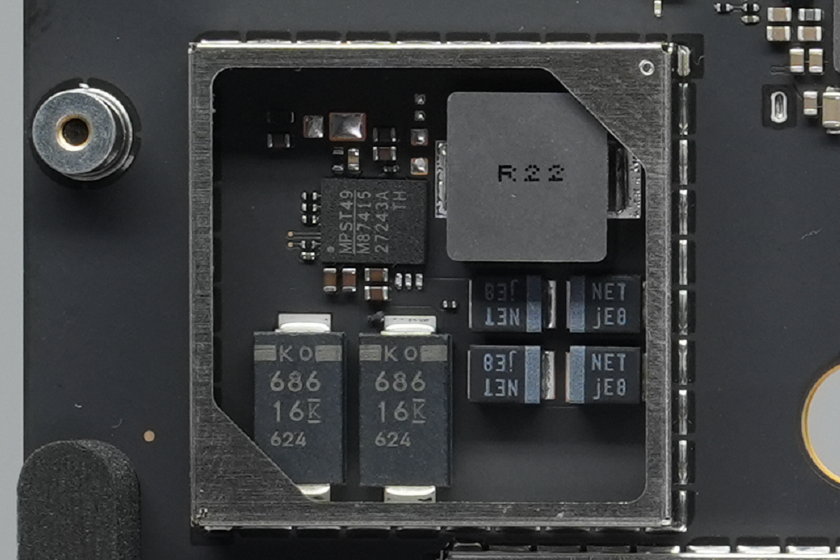
The shielding can in the upper-left section houses a PMIC, alloy inductors, and filter caps.
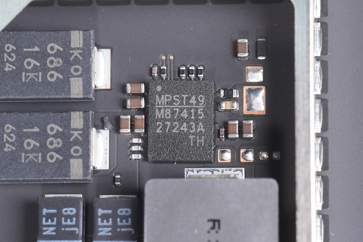
The PMIC from MPS, marked M87415.
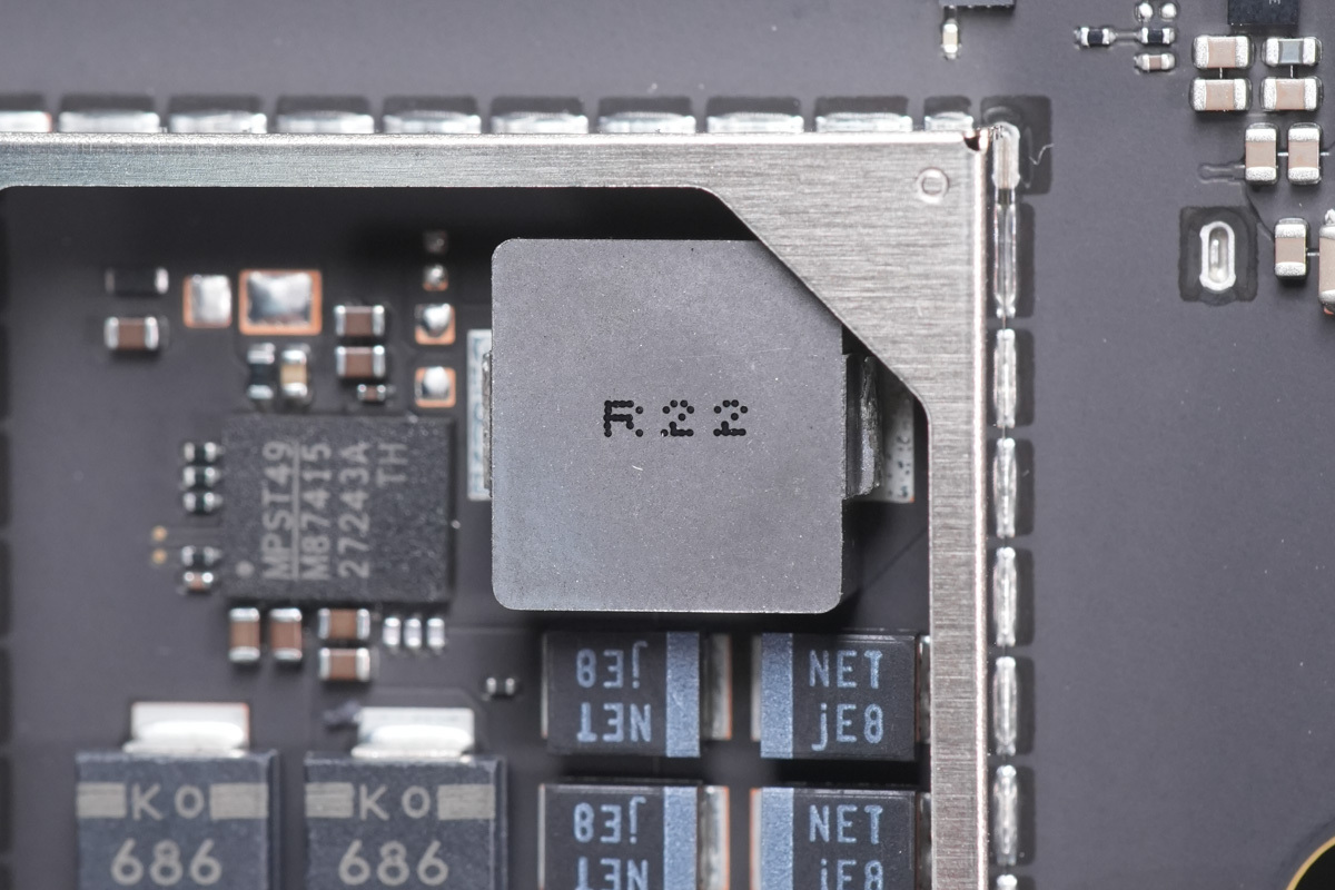
The 0.22 μH alloy inductor.
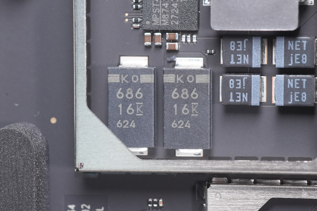
The filter caps are from KEMET, rated at 68 μF, 16 V.
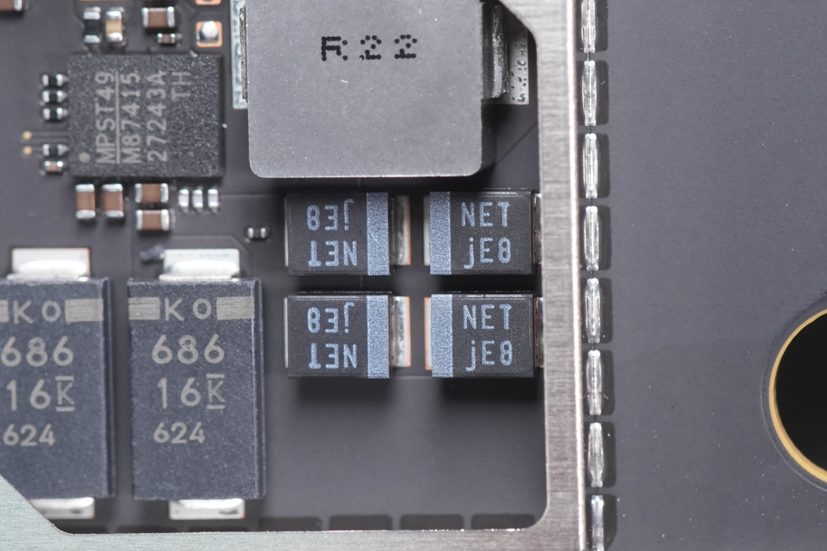
The filter caps are from KEMET, rated at 150 μF, 6.3 V.
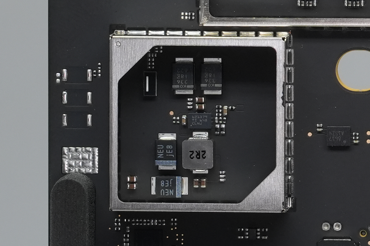
The shielding can in the lower-left section houses a buck converter chip, a buck inductor, and filter caps.
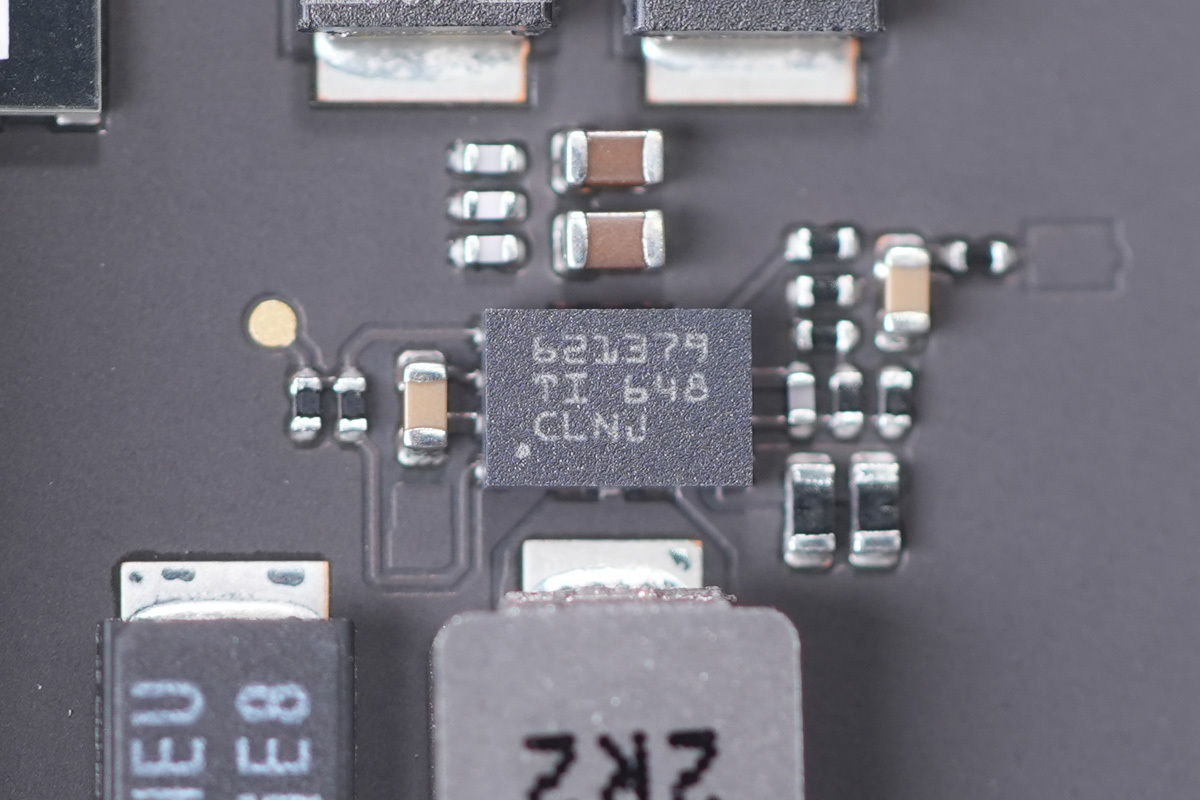
The synchronous buck converter chip is from TI, marked 621379.
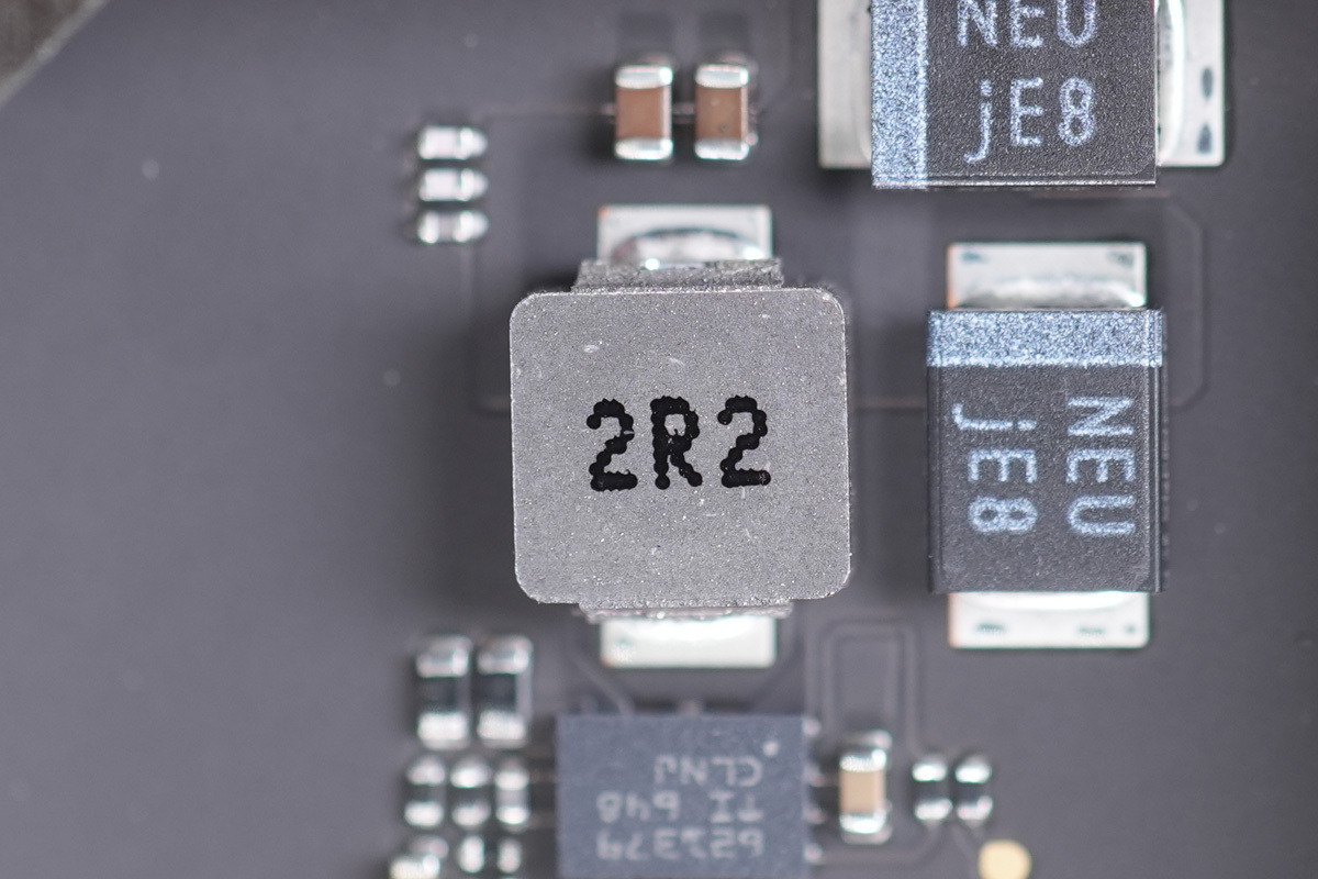
The 2.2 μH buck inductor.
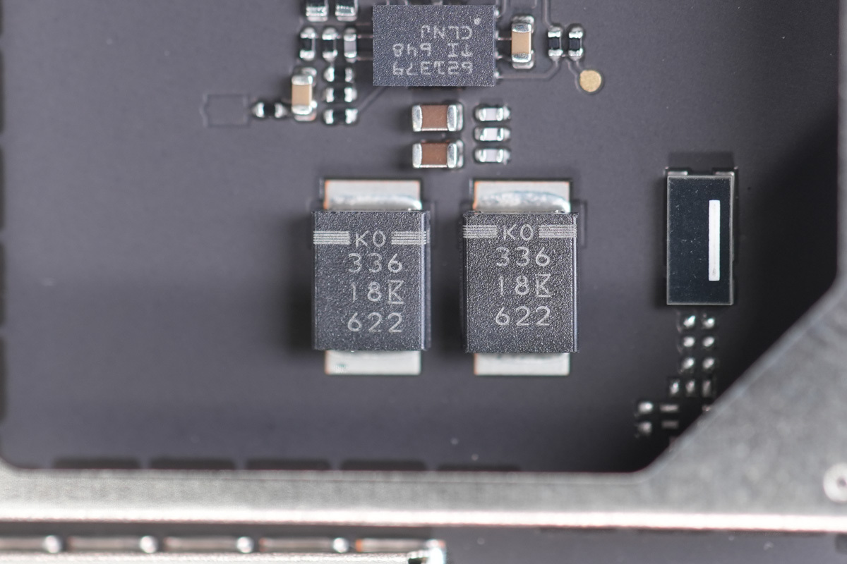
The filter cap is from KEMET, rated at 33 μF, 16 V.
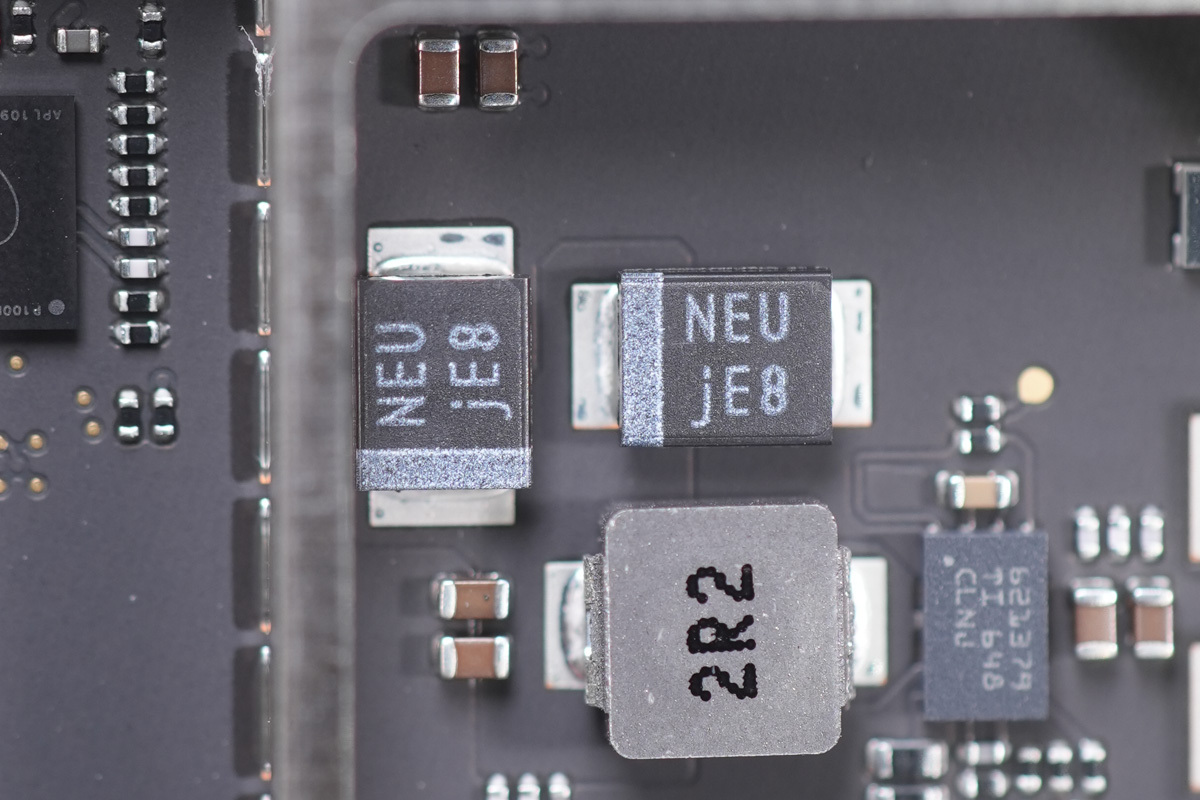
The filter cap is rated at 150 μF, 6.3 V.
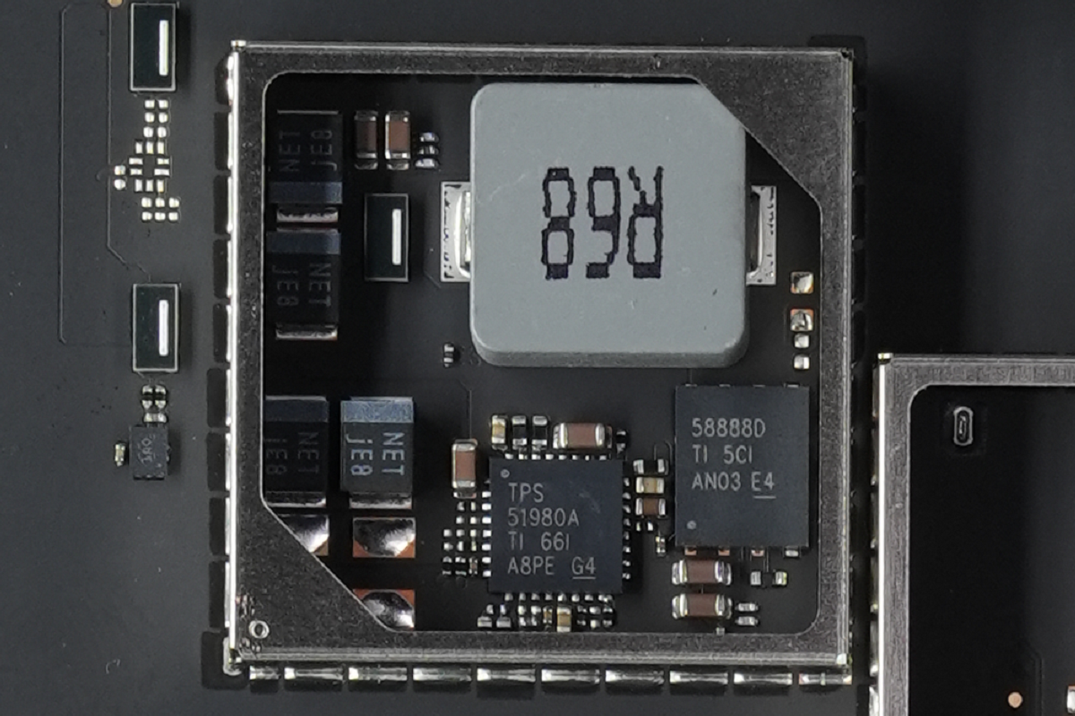
The small shielding can in the upper-right section houses a synchronous buck controller, switching MOSFETs, a buck inductor, and filter caps.
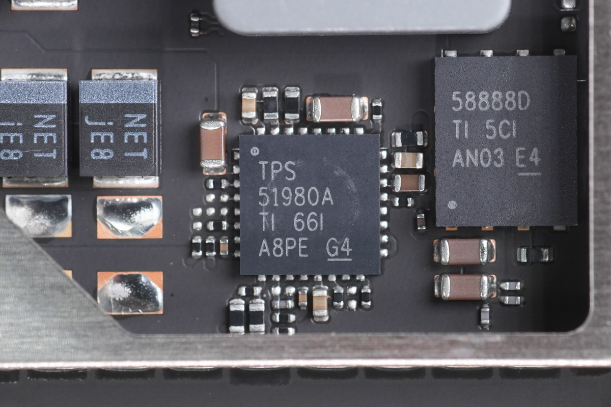
The synchronous buck controller is from TI, marked TPS51980A, and is housed in a QFN-32 package.
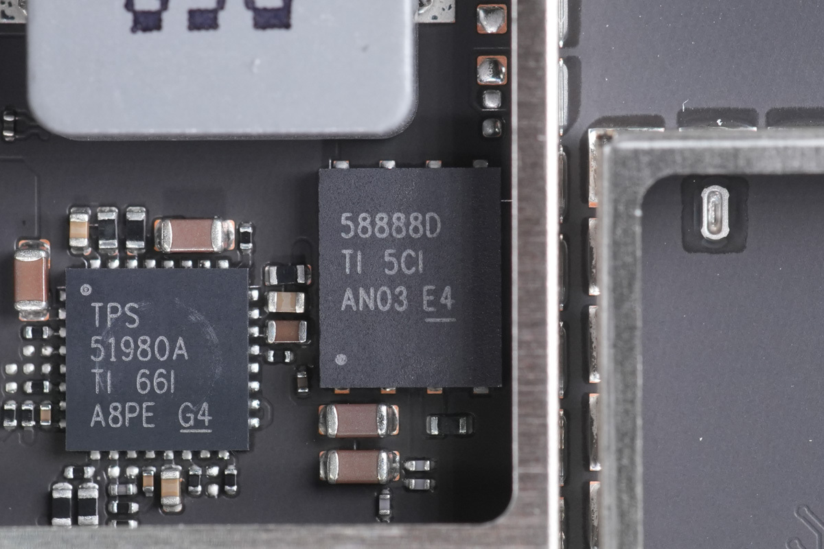
The synchronous buck switching MOSFET is from TI, marked 58888D.
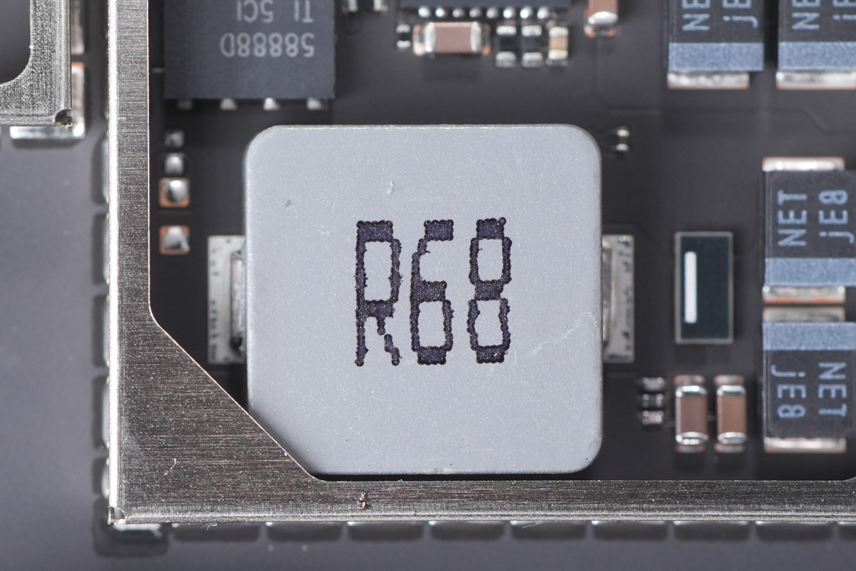
The 0.68 μH buck inductor.
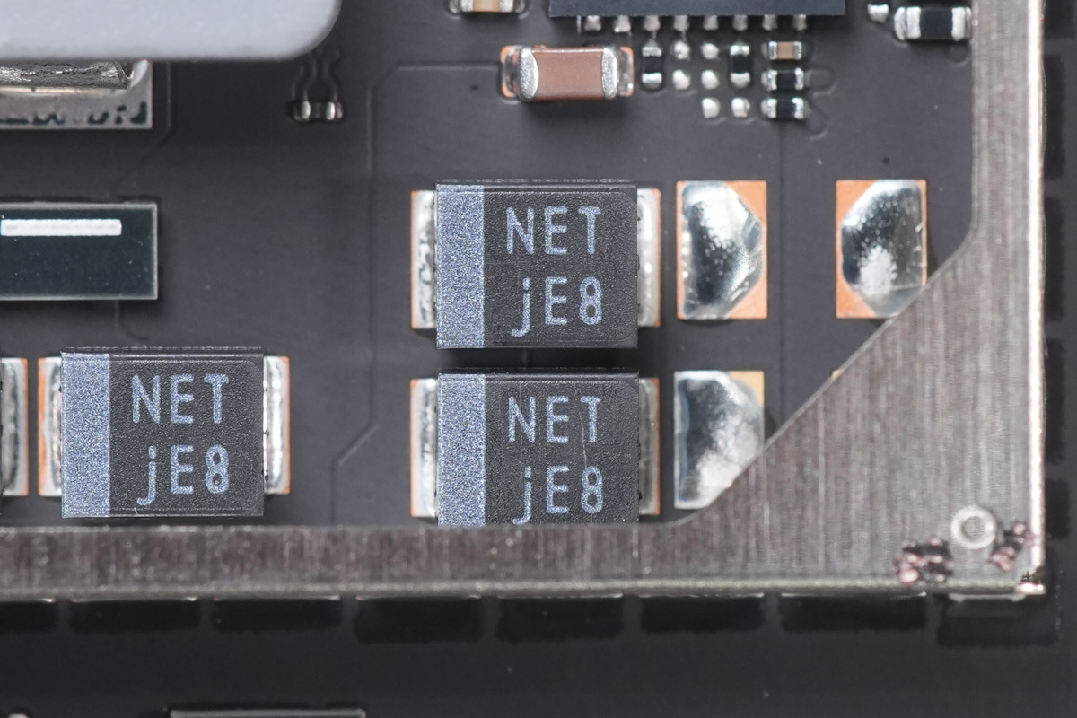
The filter cap is rated at 150 μF, 6.3 V.
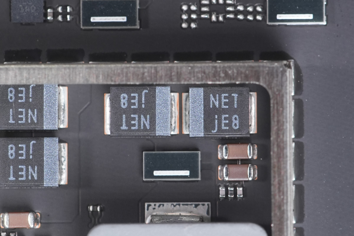
Both filter caps share the same specs.
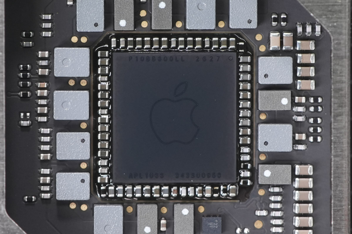
The shielding can in the lower-right section houses a PMIC marked 343S00958.
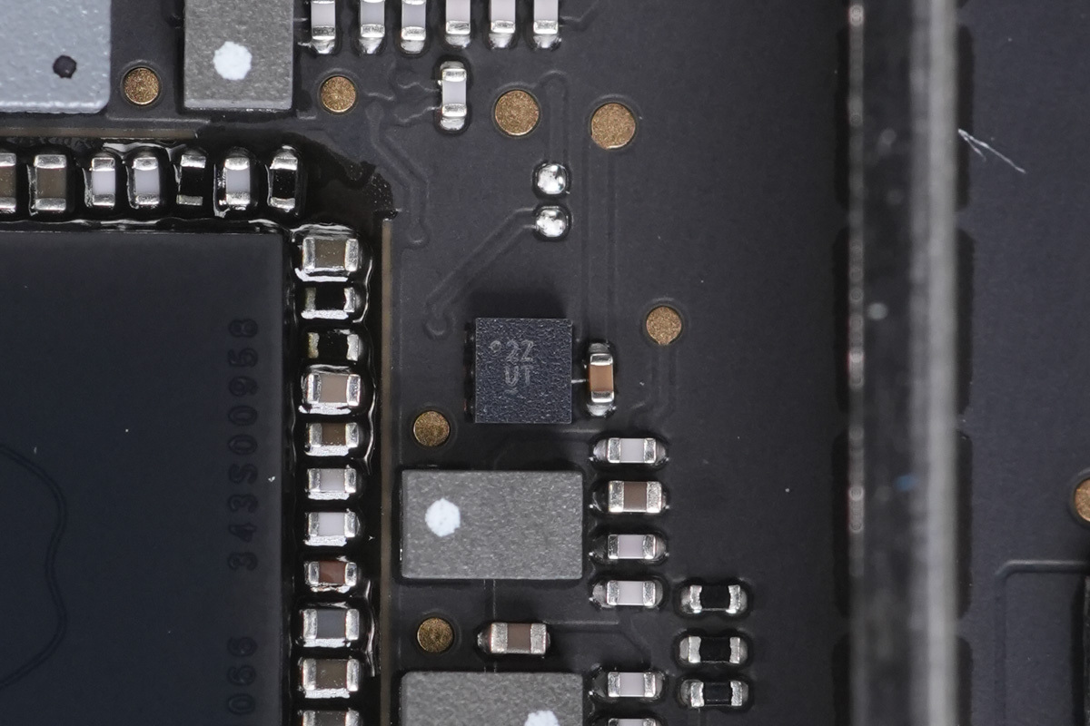
The chip marked 2Z.
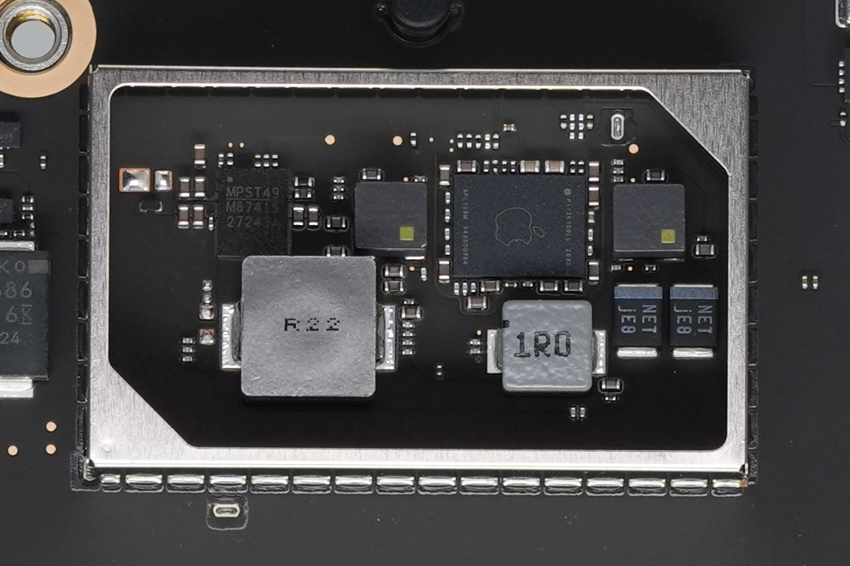
The shielding can below the chip houses a PMIC, an inductor, and filter caps.
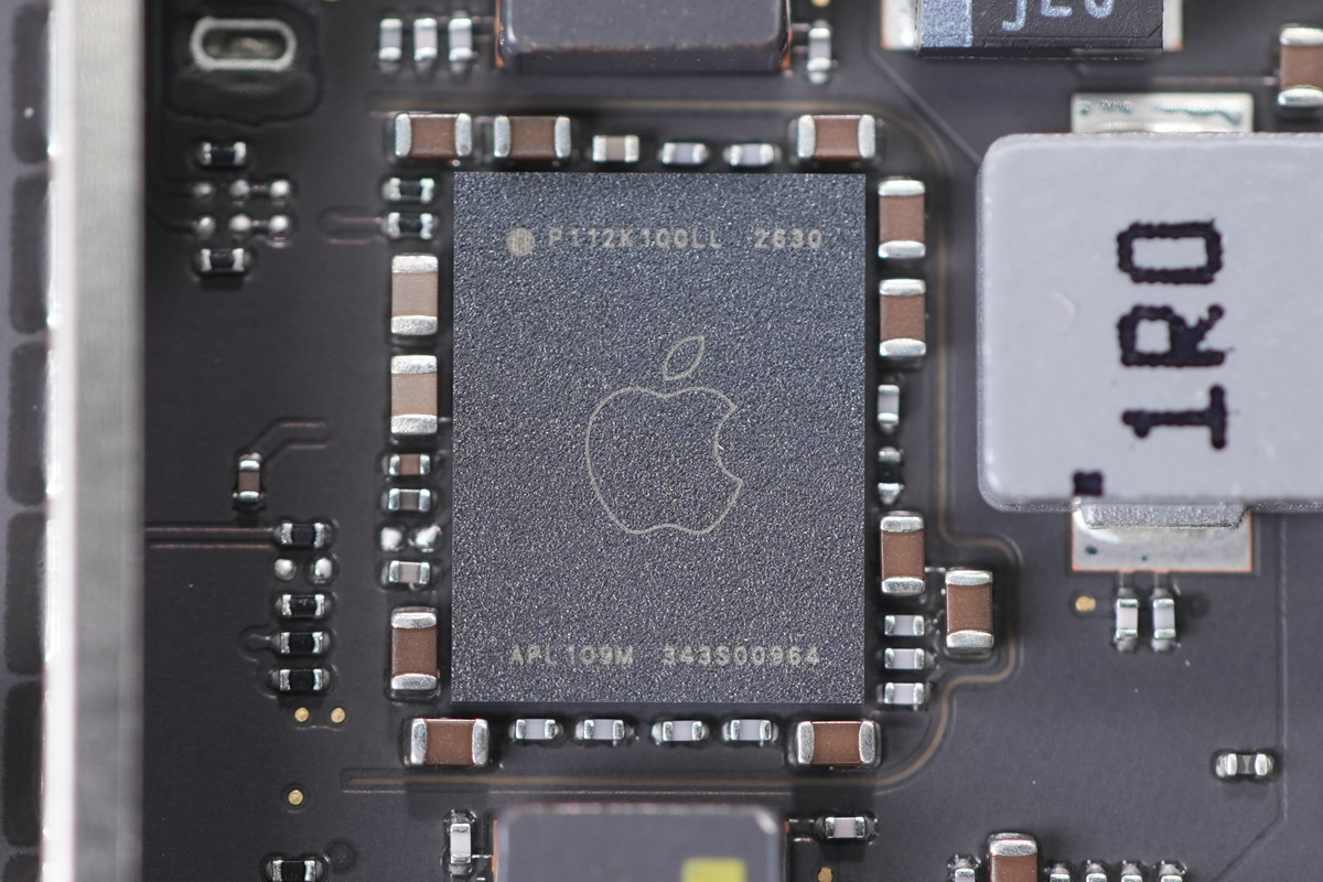
The PMIC marked 343S00964.
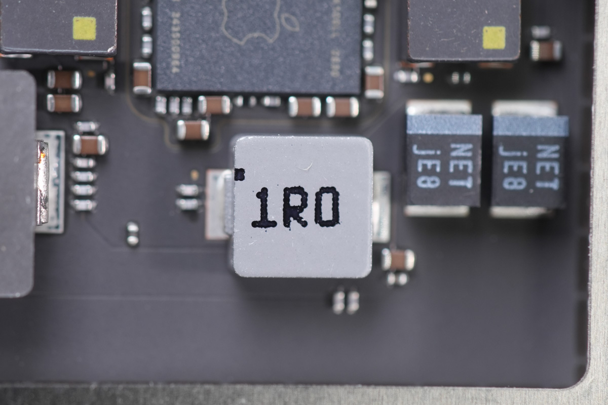
The 1 μH alloy inductor.
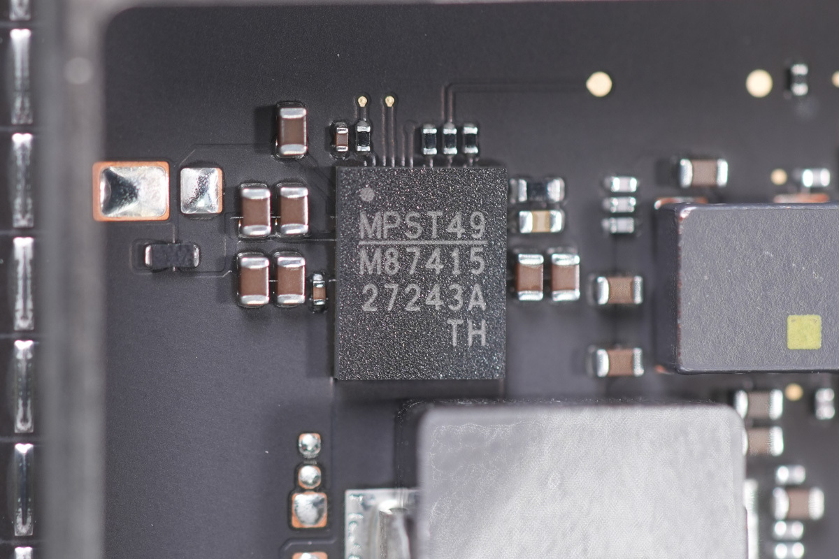
The PMIC marked M87415.
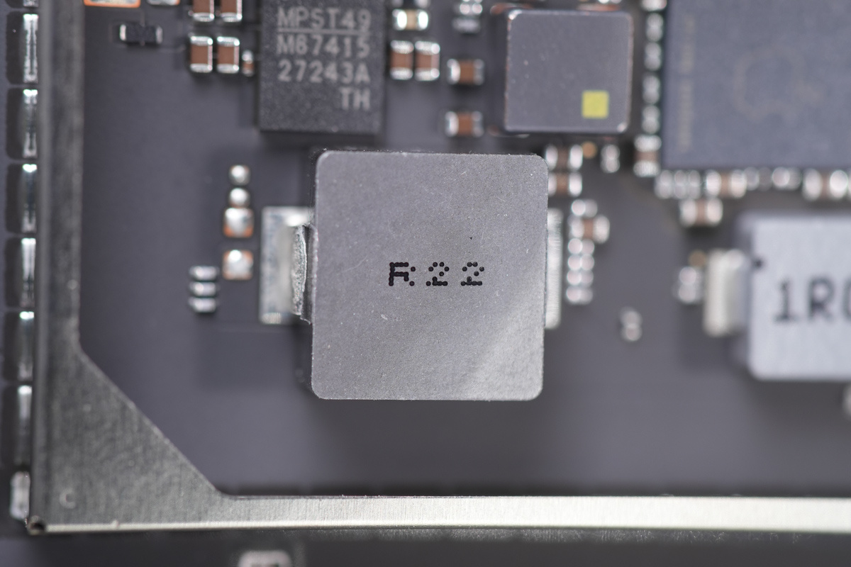
The 0.22 μH buck inductor.
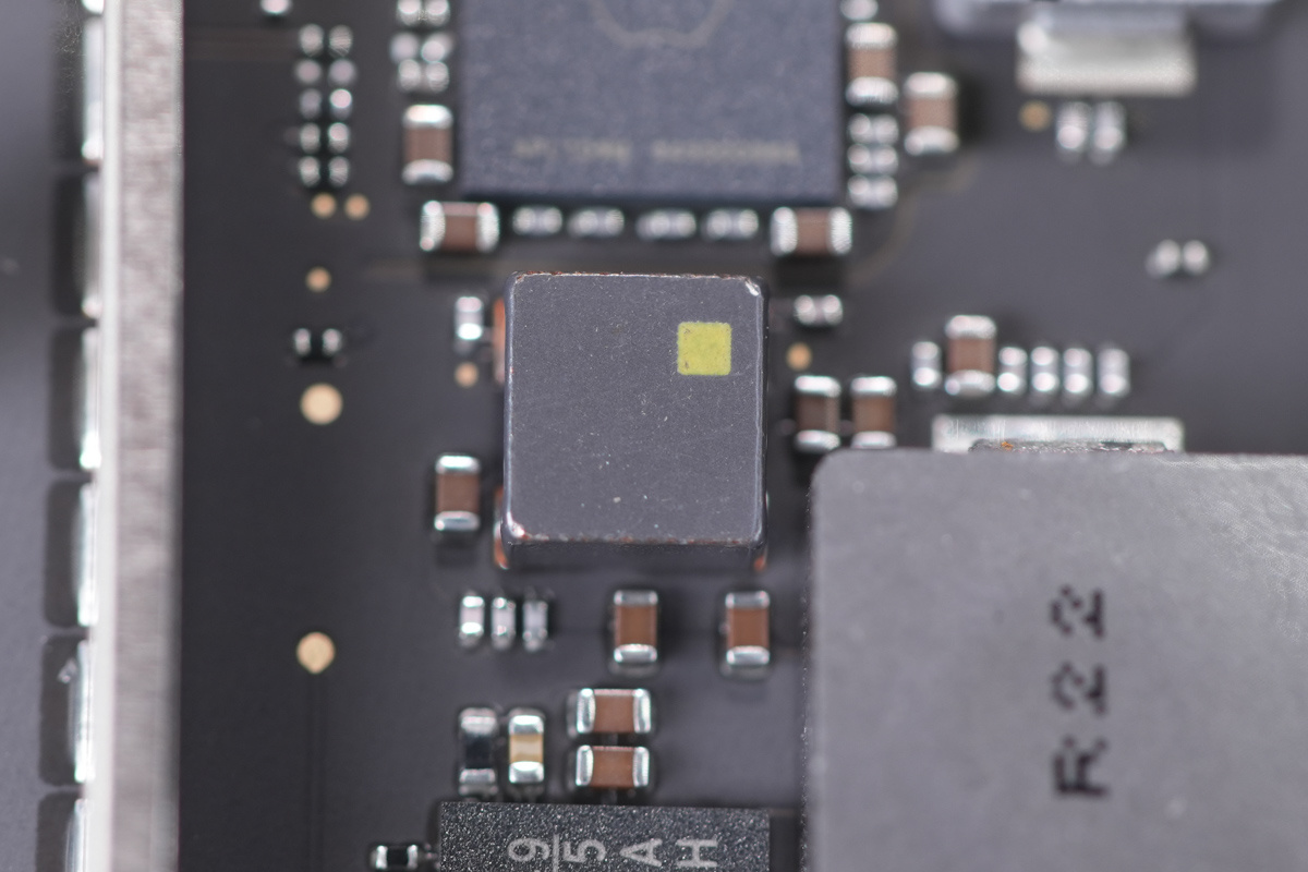
The SMD inductor.
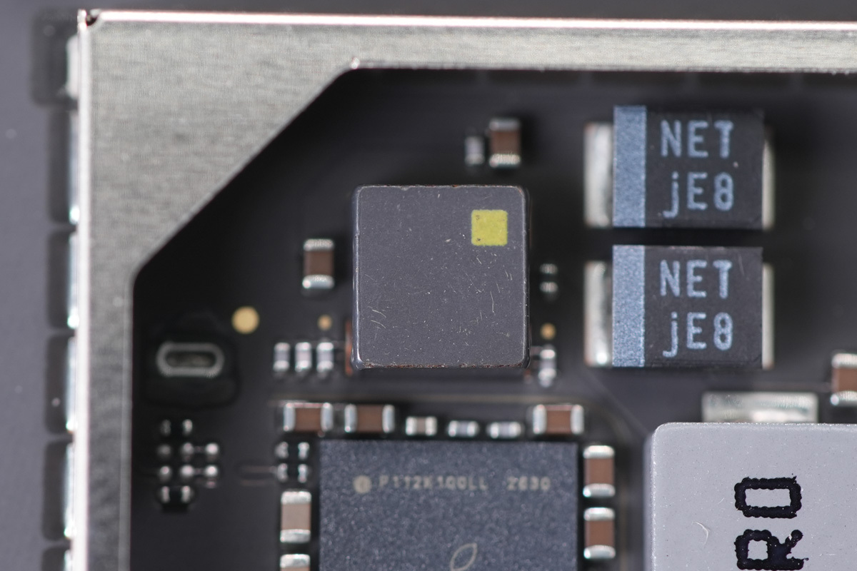
Another SMD inductor.
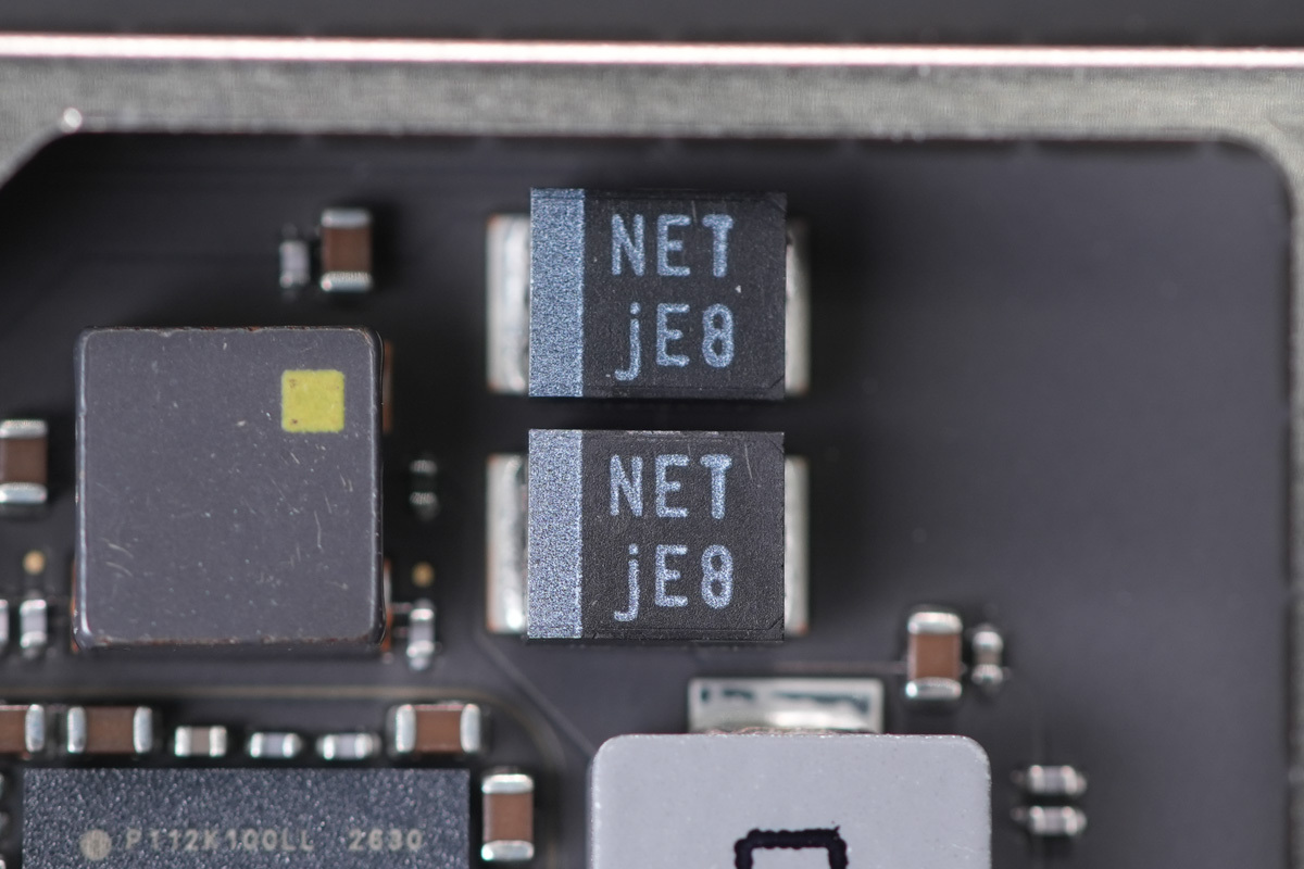
The filter cap is rated at 150 μF, 6.3 V.
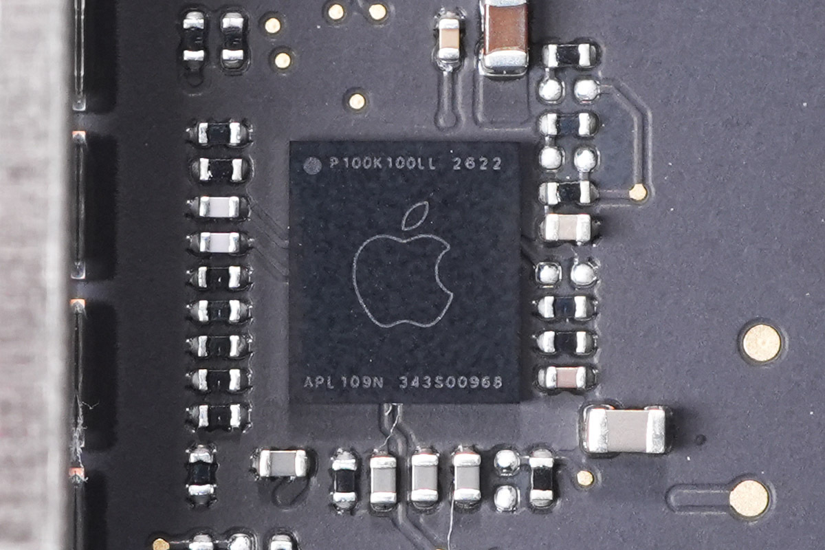
A chip outside the shielding can is marked 343S00968.
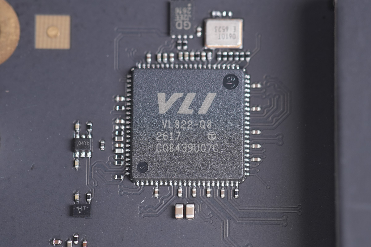
The USB hub controller is from VLI, model VL822-Q8. It integrates an upstream port and two downstream-port multiplexers, supports expansion for two USB-A and two USB-C ports, supports data rates up to 10 Gbps, and is housed in a QFN-88 package.
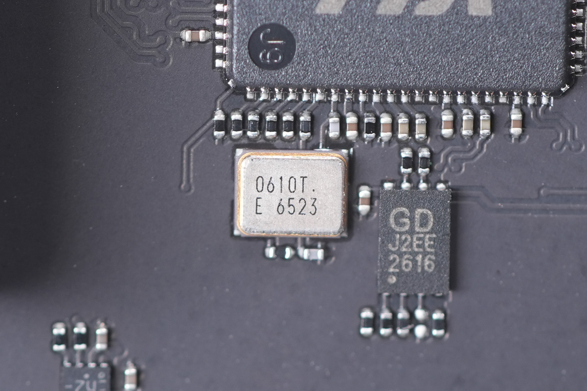
The external clock crystal for the chip.
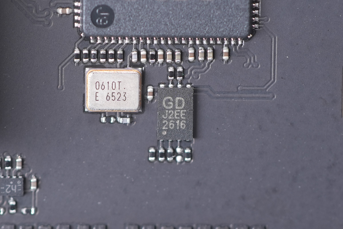
The memory chip is from GigaDevice, marked J2EE.
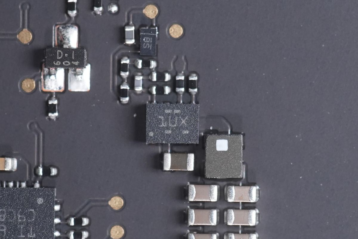
The buck converter chip marked 1UX.
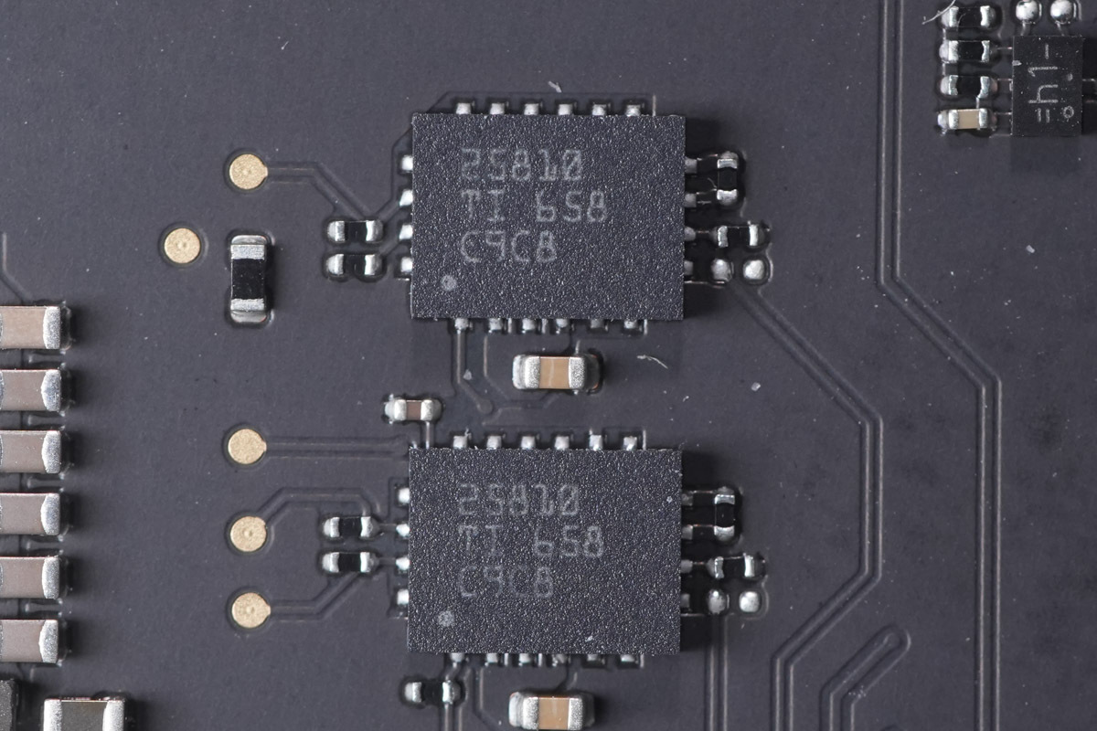
The USB-C power switch is from TI, model TPS25810, which provides power control for the USB-C port, supports VCONN power, and is housed in a WQFN-20 package.
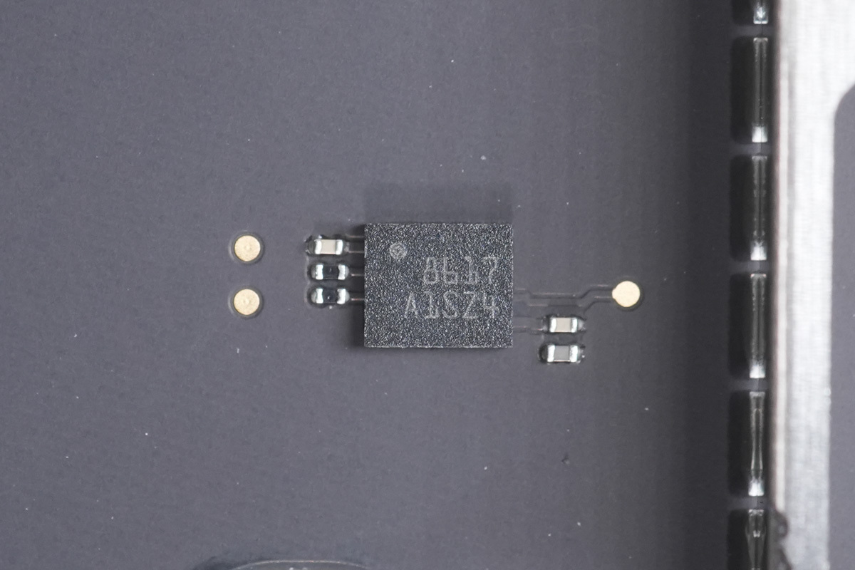
The chip marked A1SZ4.
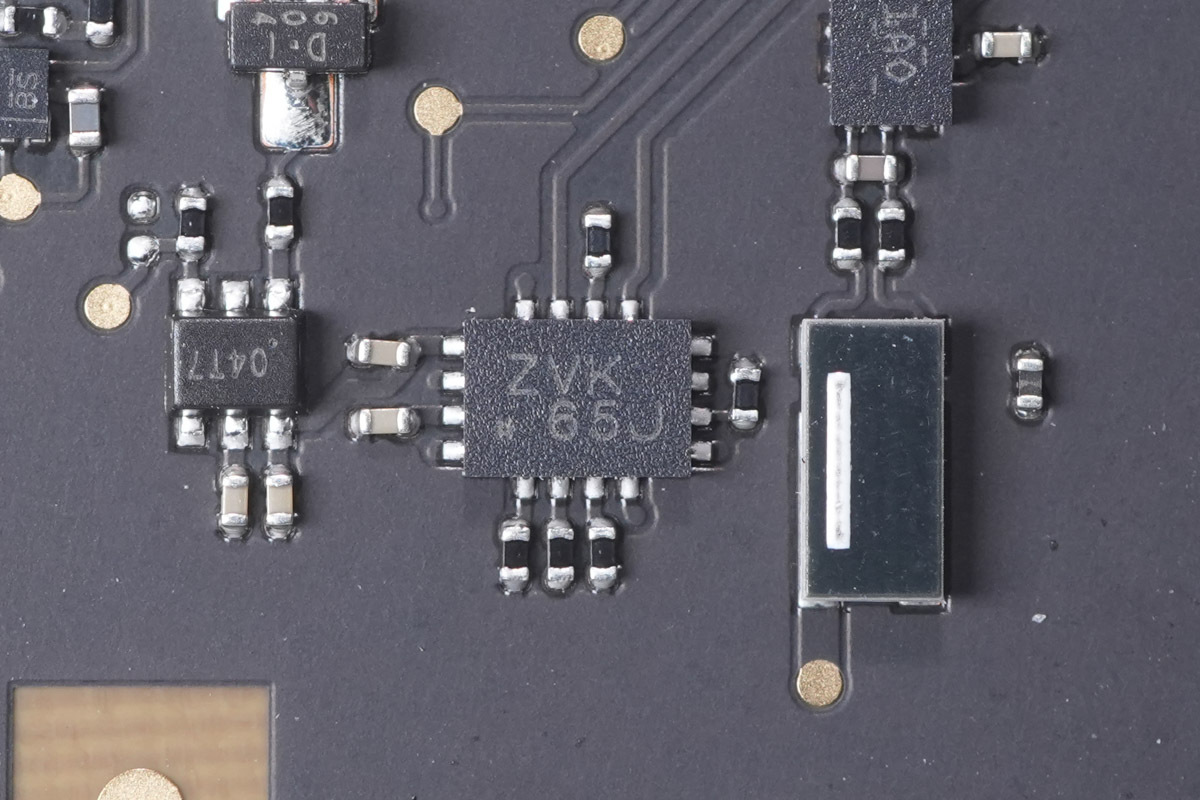
The chip marked ZVK.
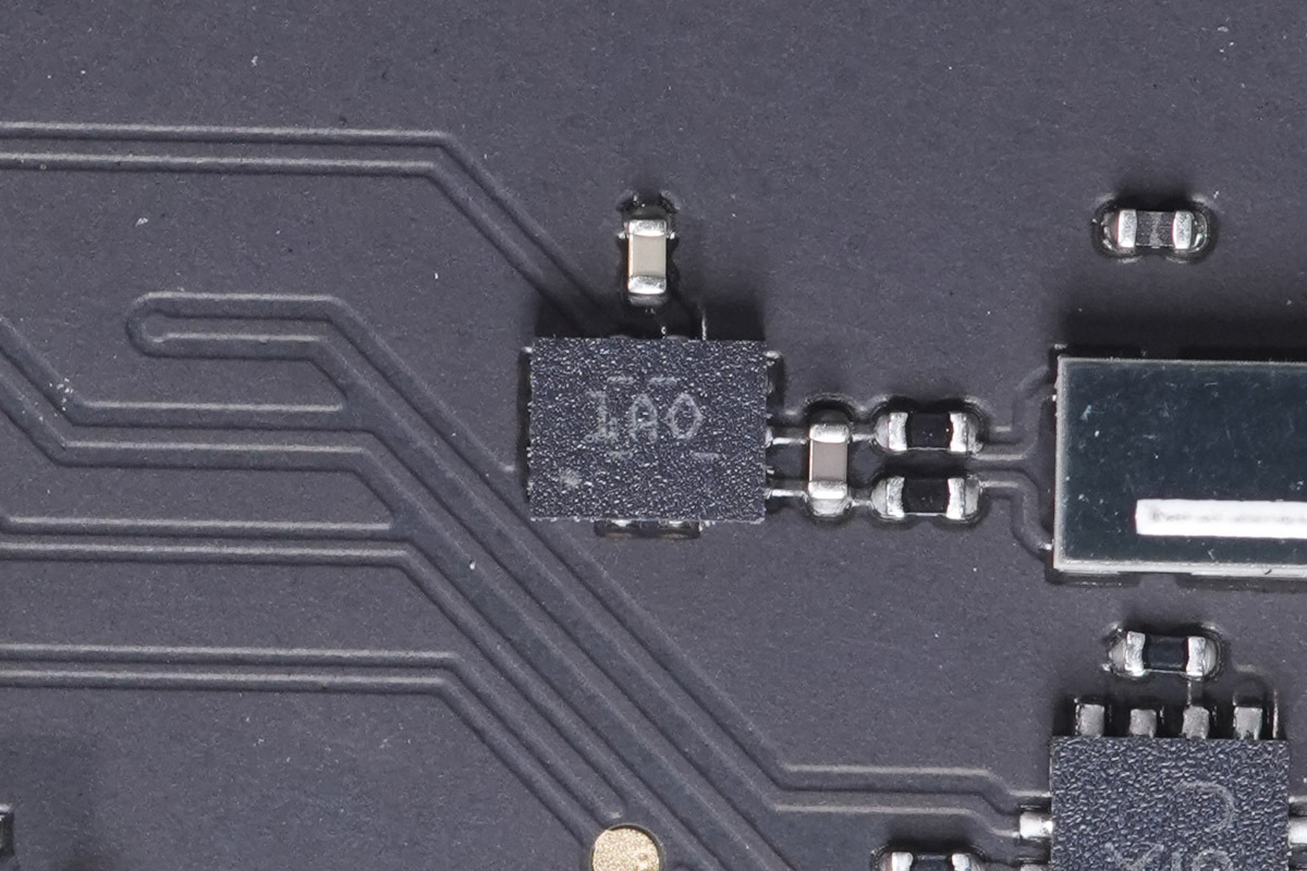
The current-sense amplifier is the TI INA190.
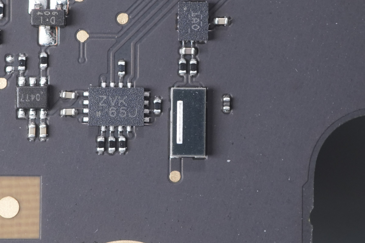
The SMD current-sense resistor.
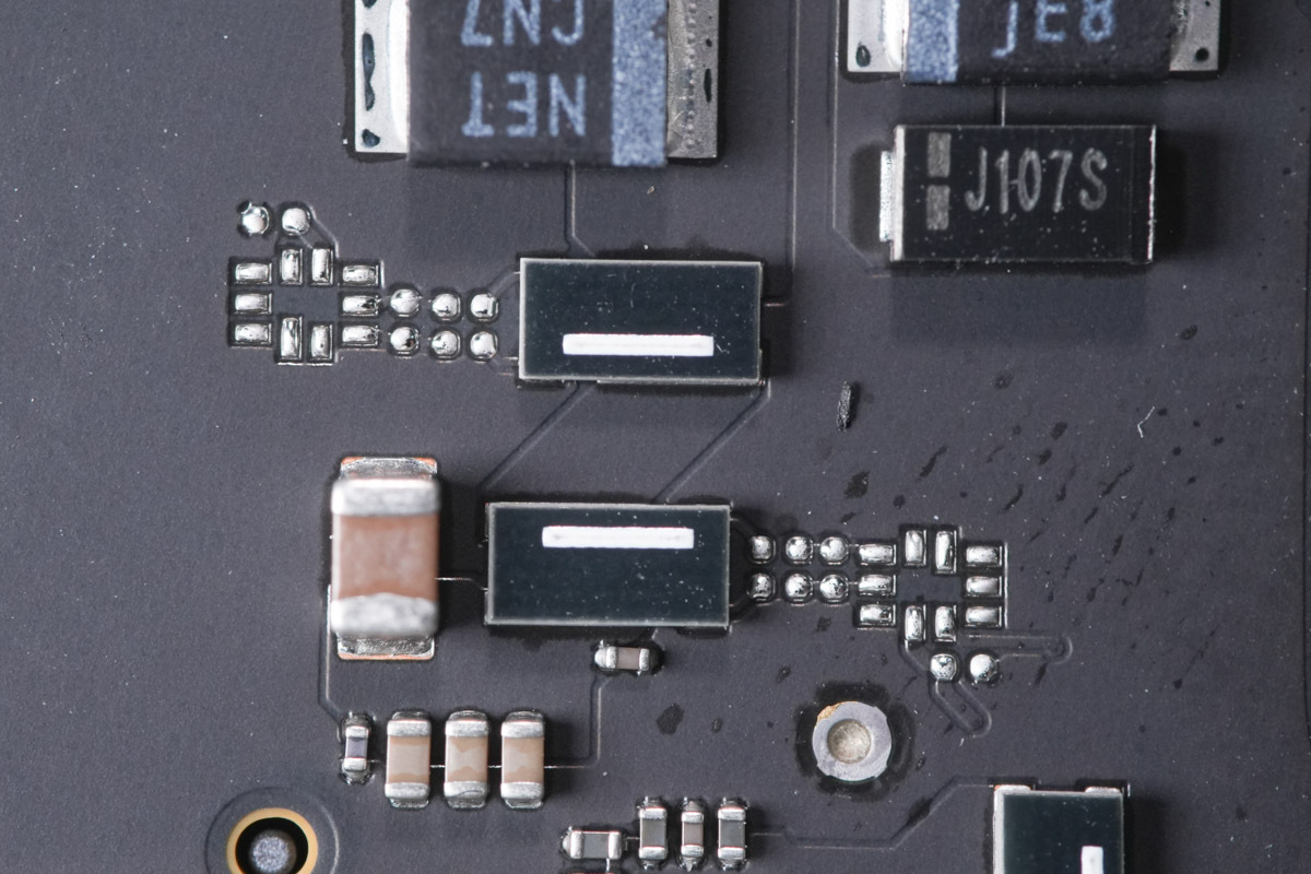
The two current-sense resistors.
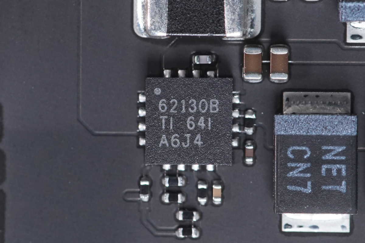
The chip marked 62130B is from TI.
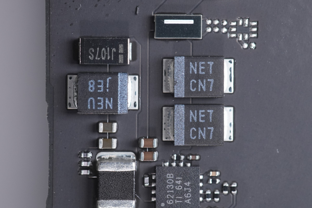
The two filter caps are rated at 33 μF, 16 V.
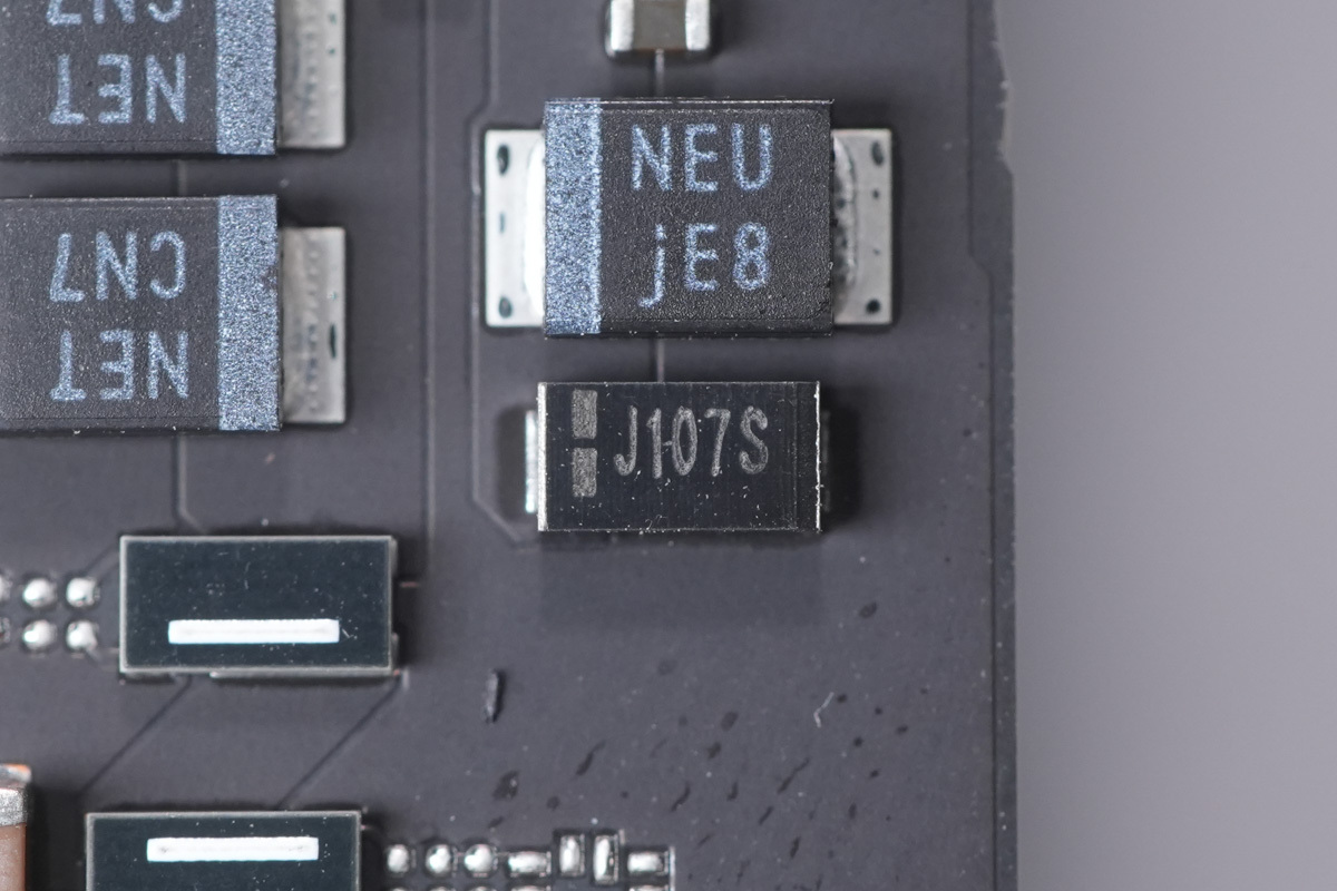
The filter caps are rated at 150 μF, 6.3 V and 100 μF, 6.3 V.
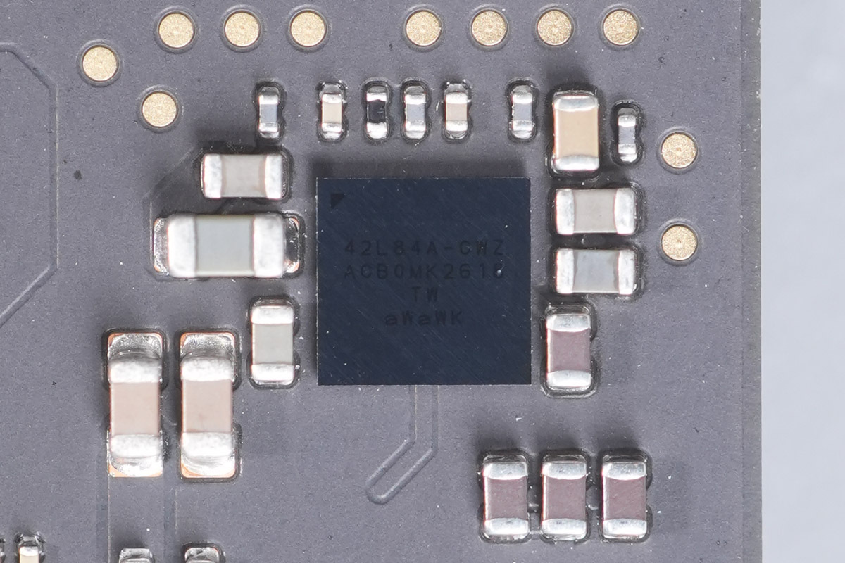
Audio chip marked 42L84A.
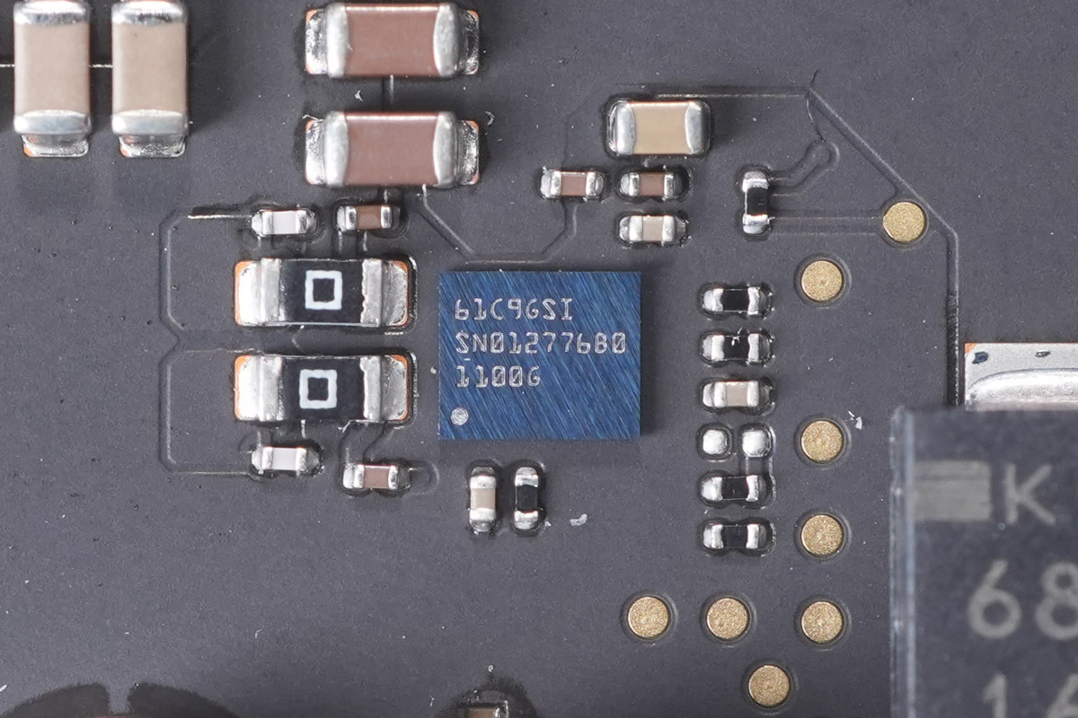
The audio amplifier chip is from TI, model SN012776B0.
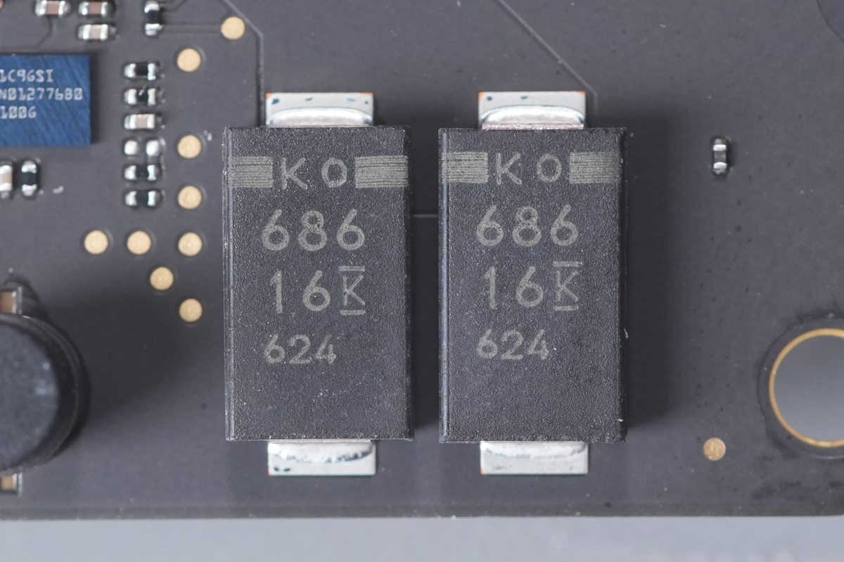
The filter cap is rated at 68 μF, 16 V.
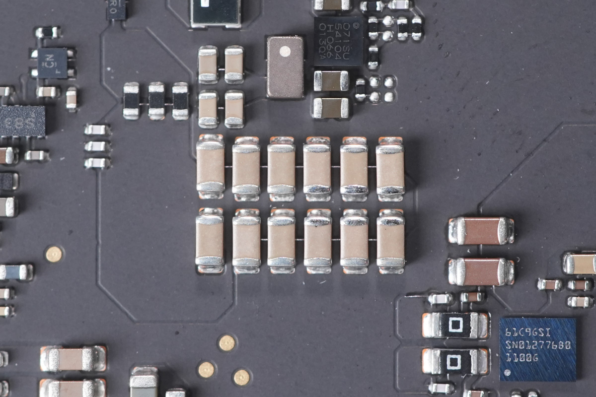
The MLCC filter caps.
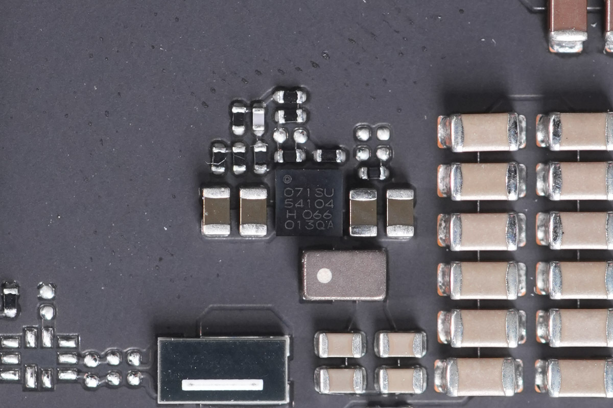
The chip marked 071SU.
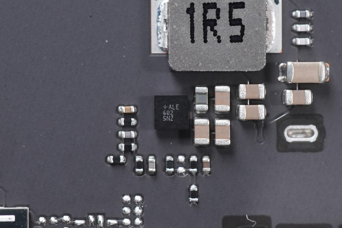
The chip marked +ALE.
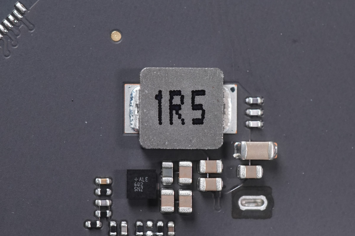
The 1.5 μH alloy inductor.
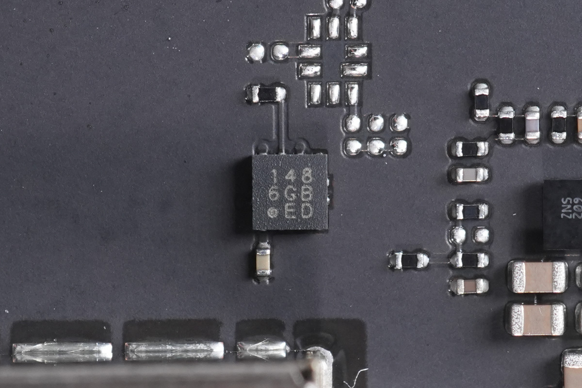
The chip marked 1486GB.
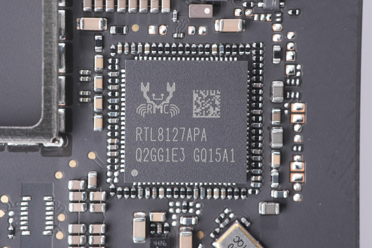
The Ethernet controller is from REALTEK, model RTL8127APA, housed in a QFN-88 package.
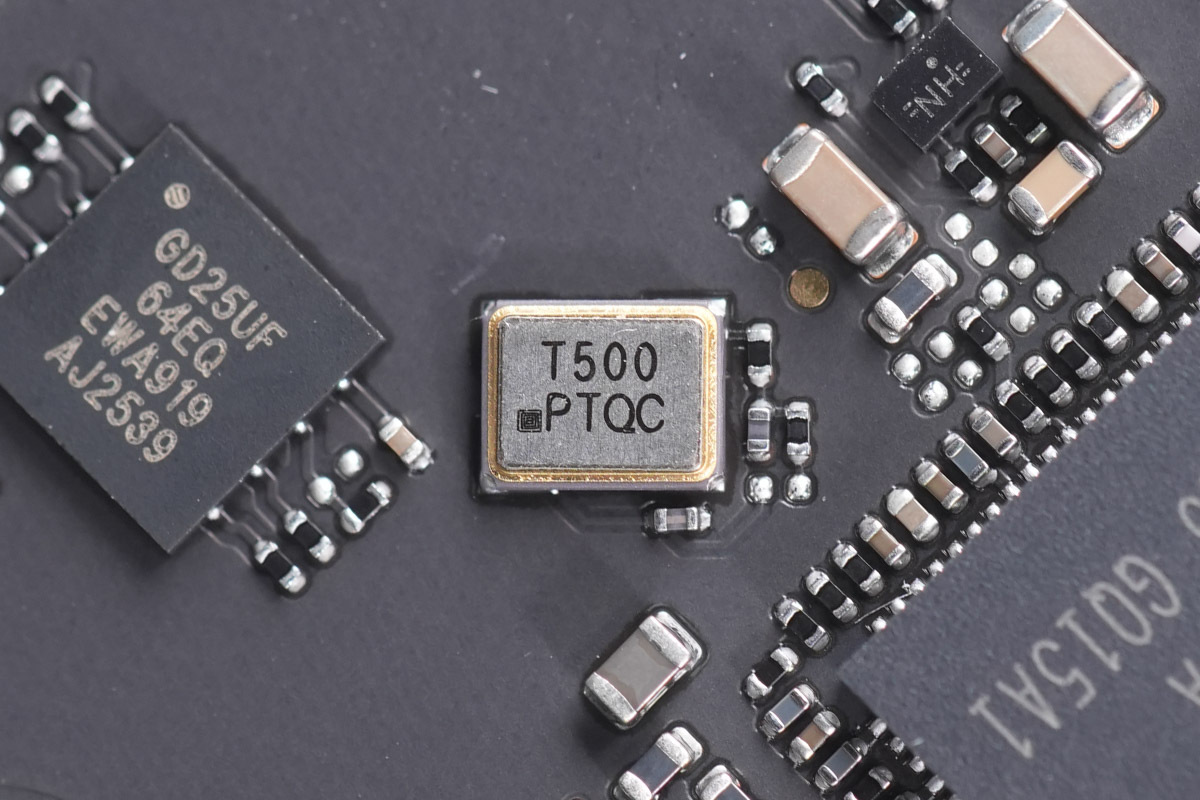
The external clock crystal.
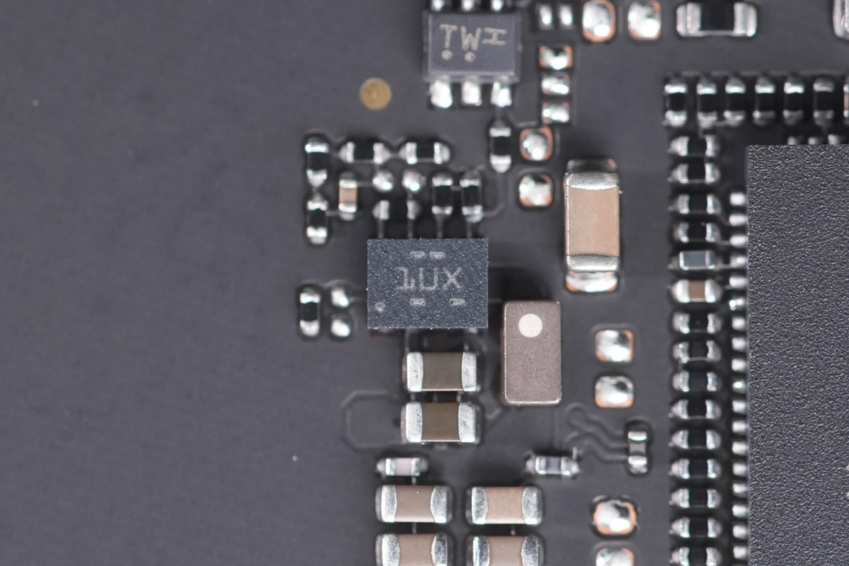
The buck converter chip marked 1UX.
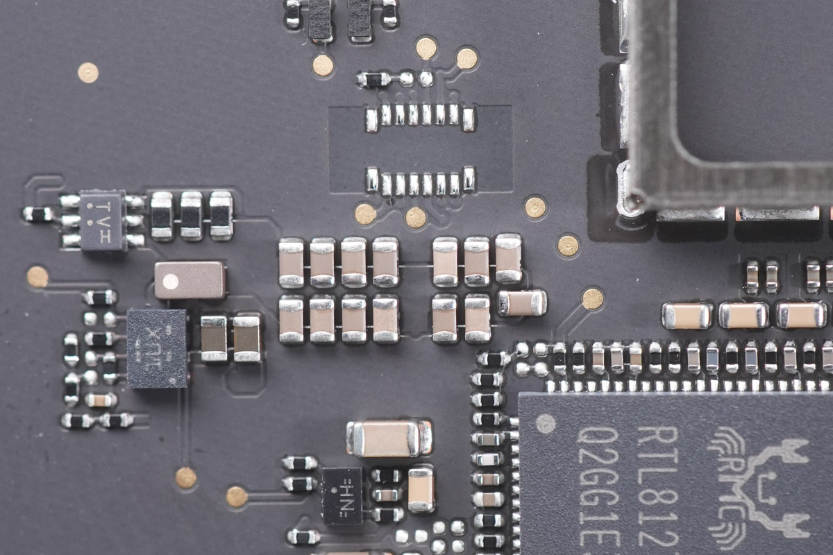
The MLCC filter caps.
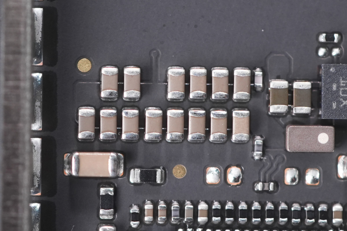
The other MLCC filter caps.
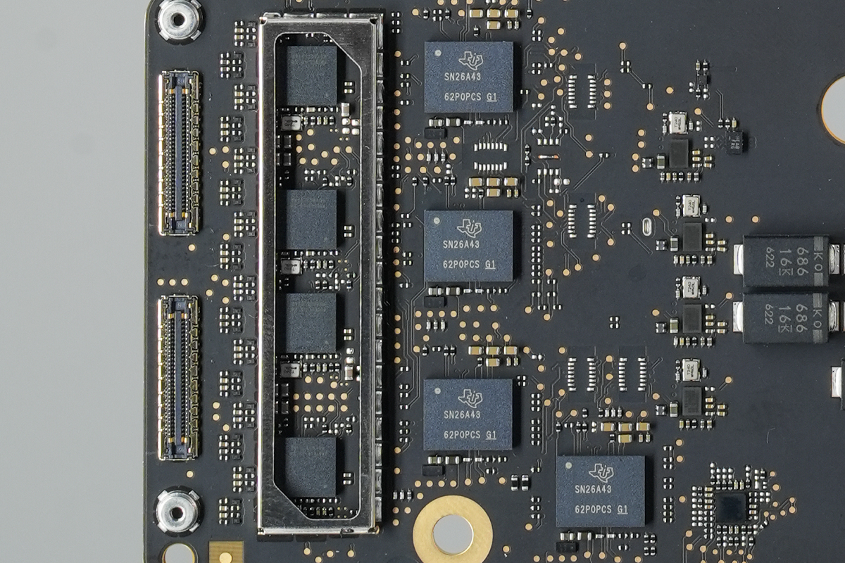
A connector is located on the left side of the shielding can. The shielding can houses a Thunderbolt controller, while a USB-C controller is located on the right.
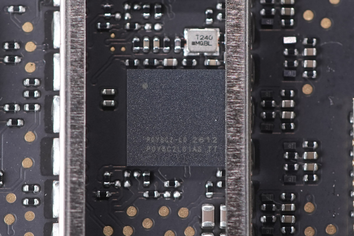
Thunderbolt controller marked P0Y5C2-L0.
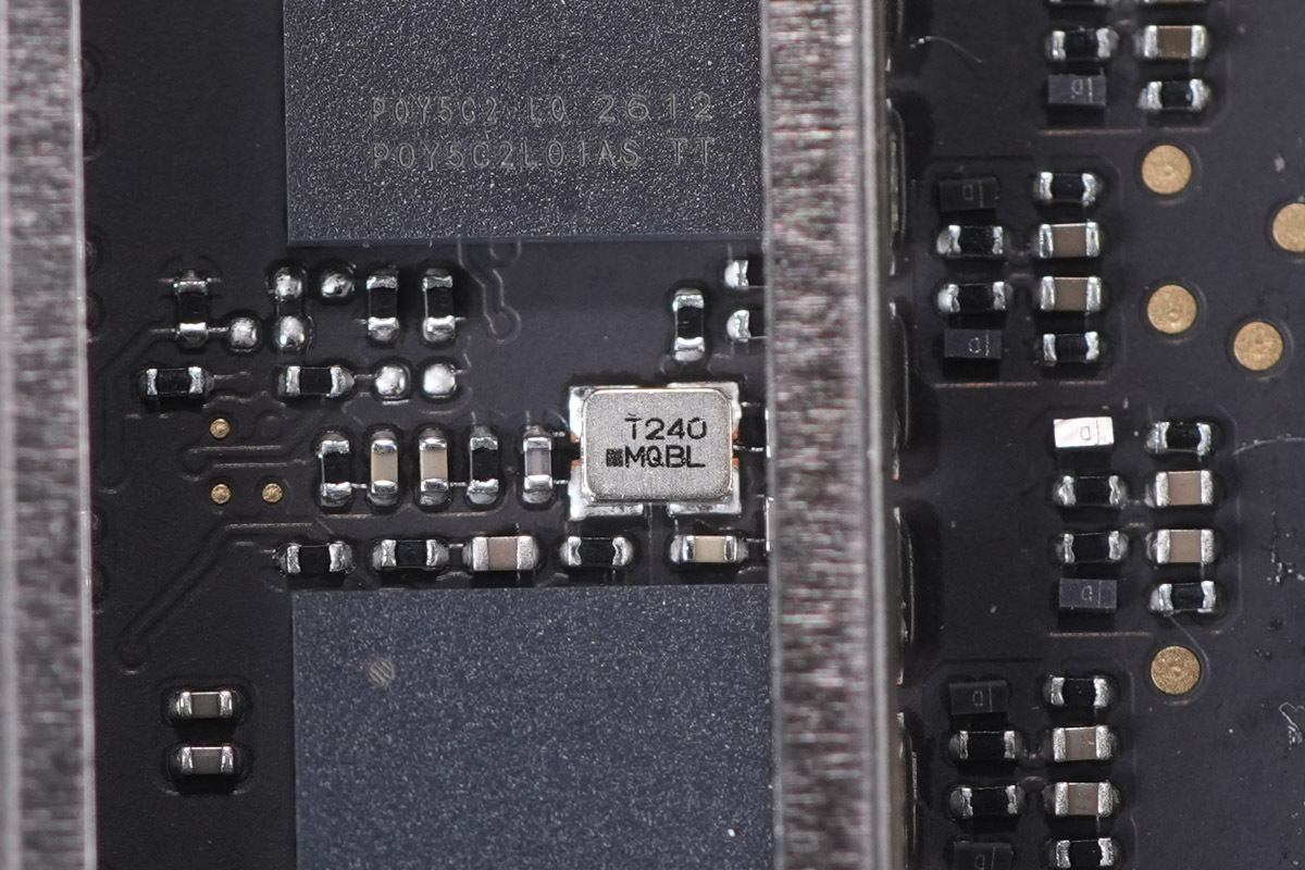
The external clock crystal.
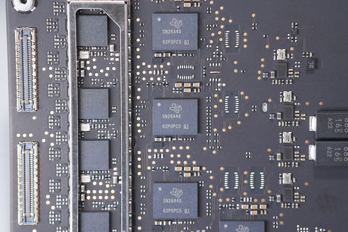
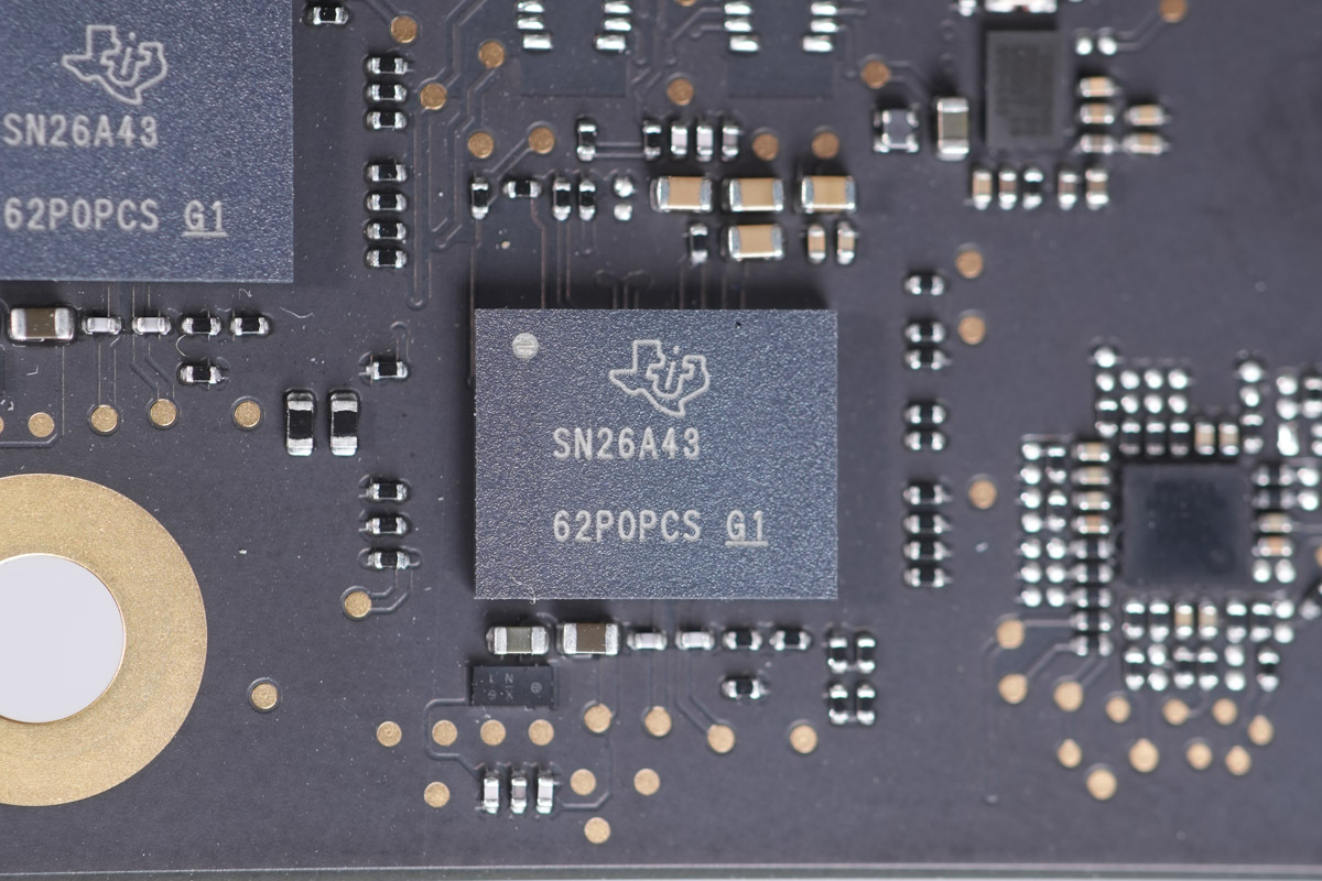
The USB-C controller is from TI, marked SN26A43.
Four chips are provided, corresponding to the four USB-C ports.
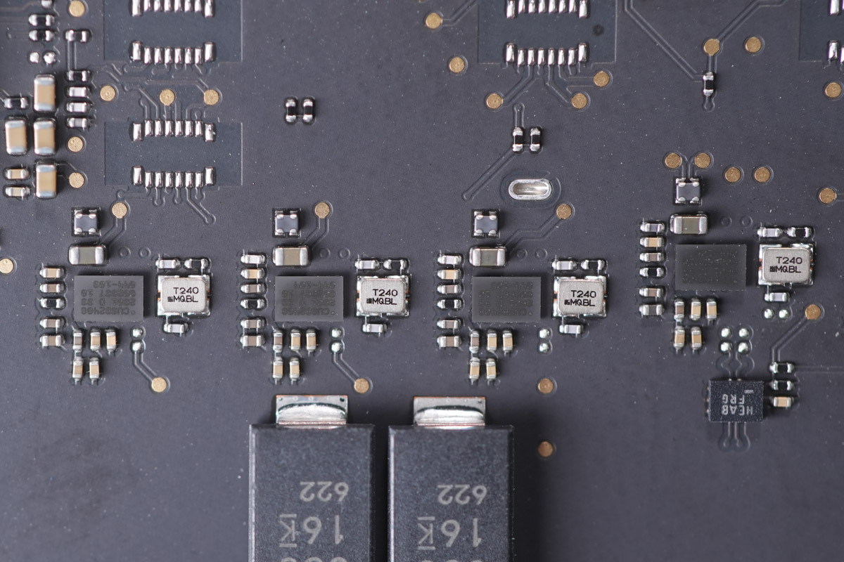
Four CUSB2408 chips are located on one side.
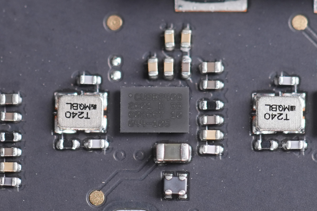
The chip marked CUSB2408.
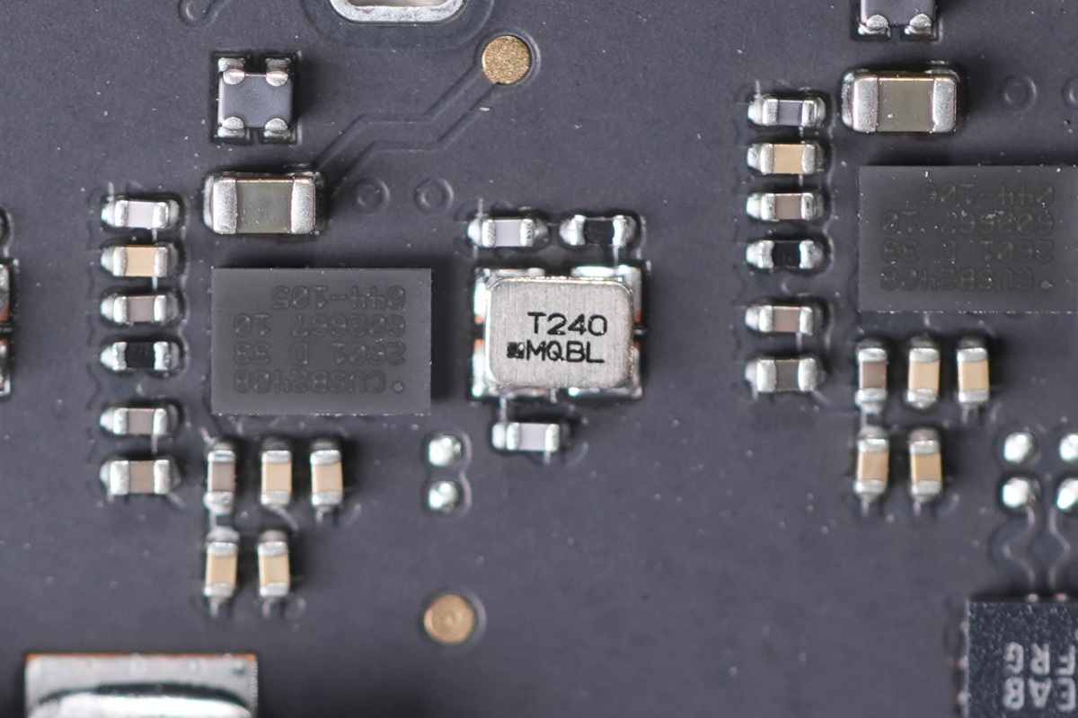
A clock crystal is located beside the chip.
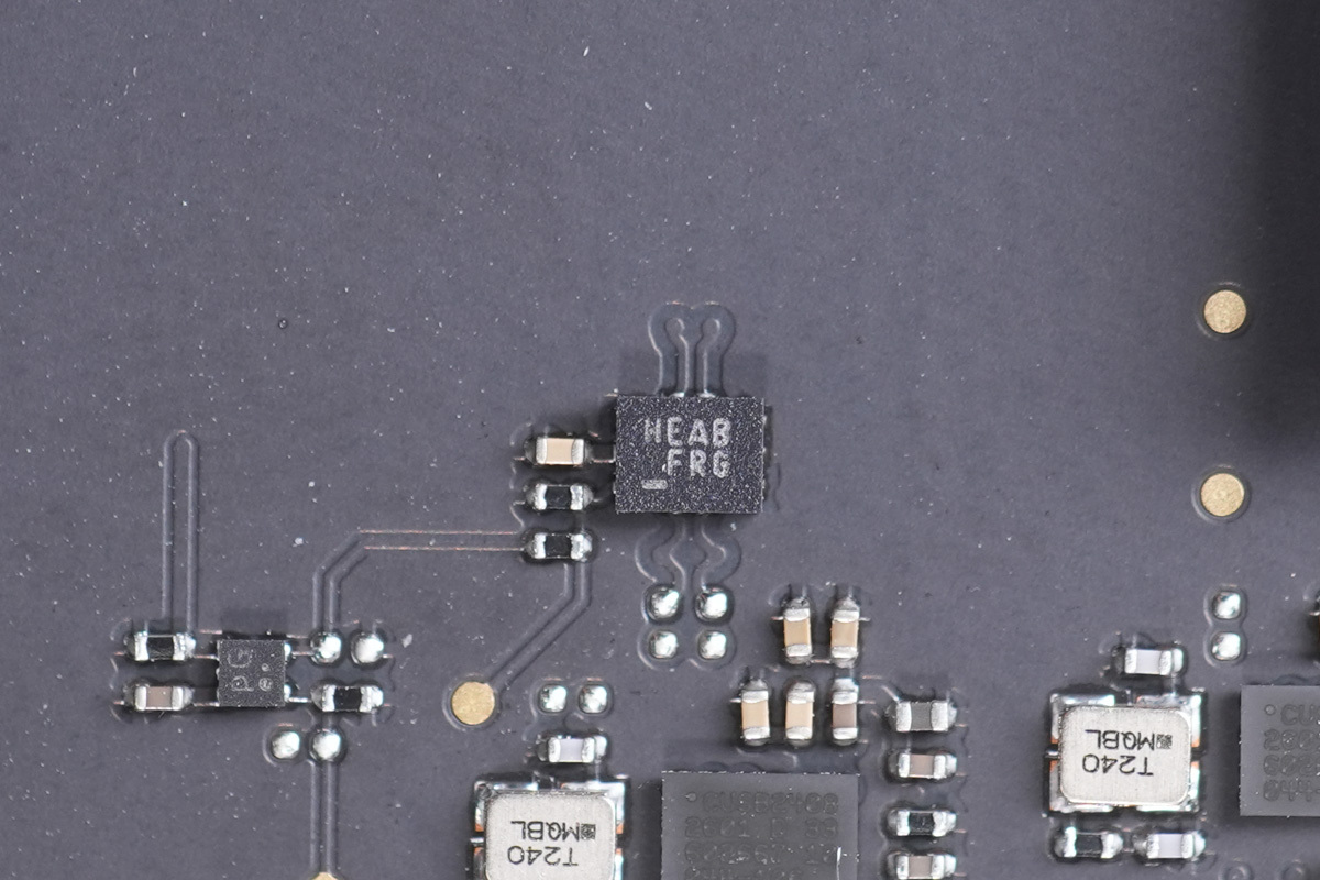
The chip marked HEAB.
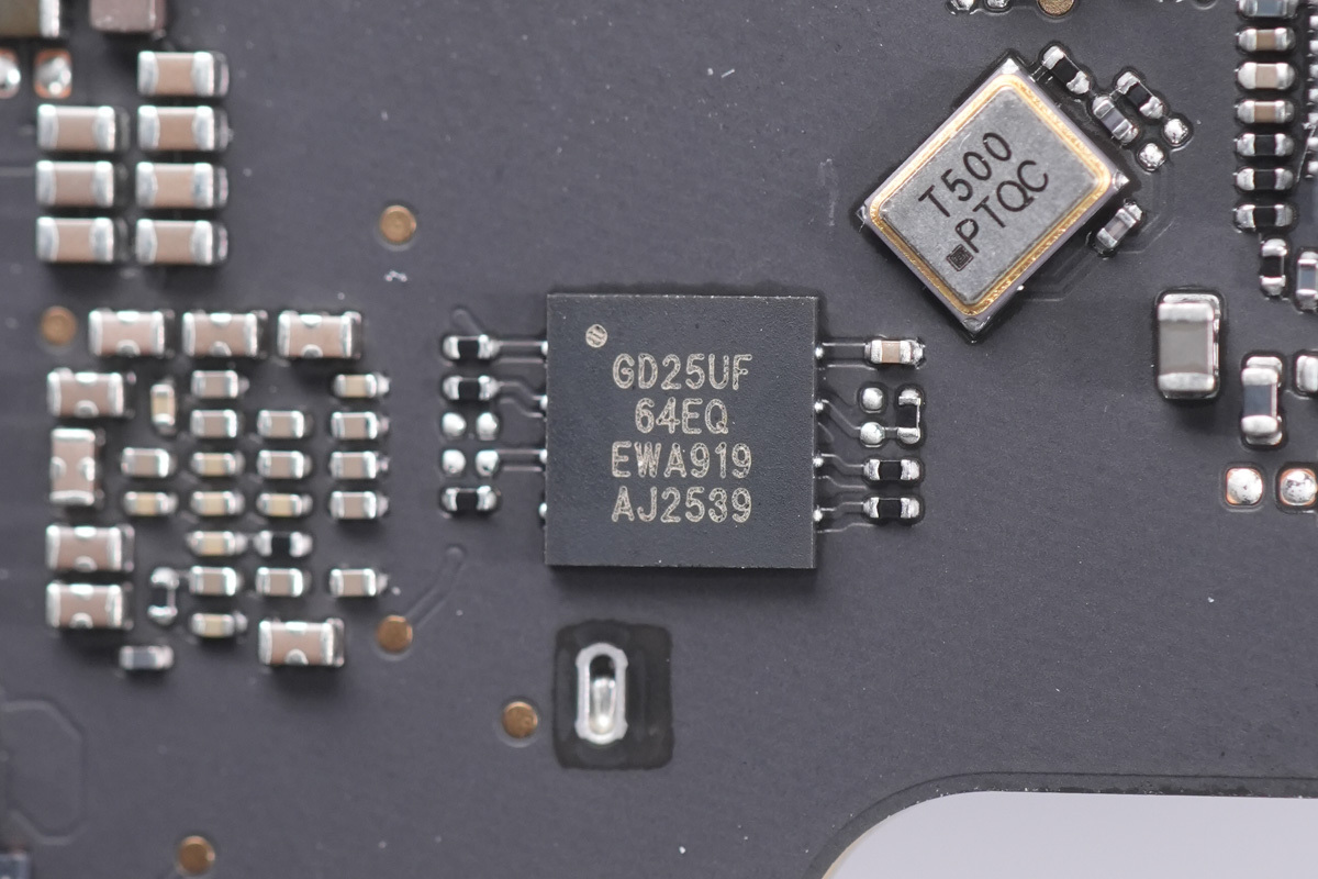
The memory chips are GigaDevice GD25UF64E devices, with four chips provided for the four USB-C ports.
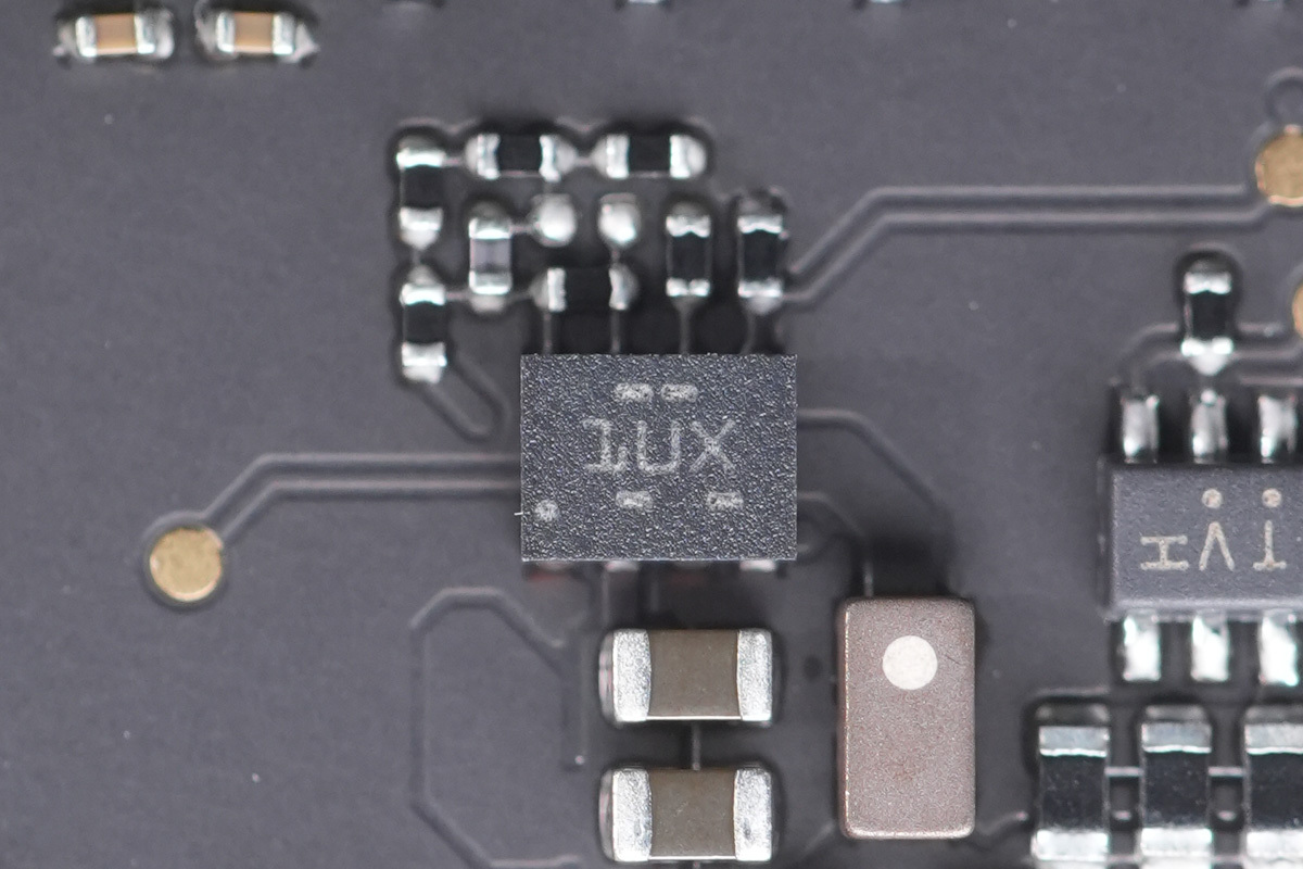
The buck converter chip marked 1UX.
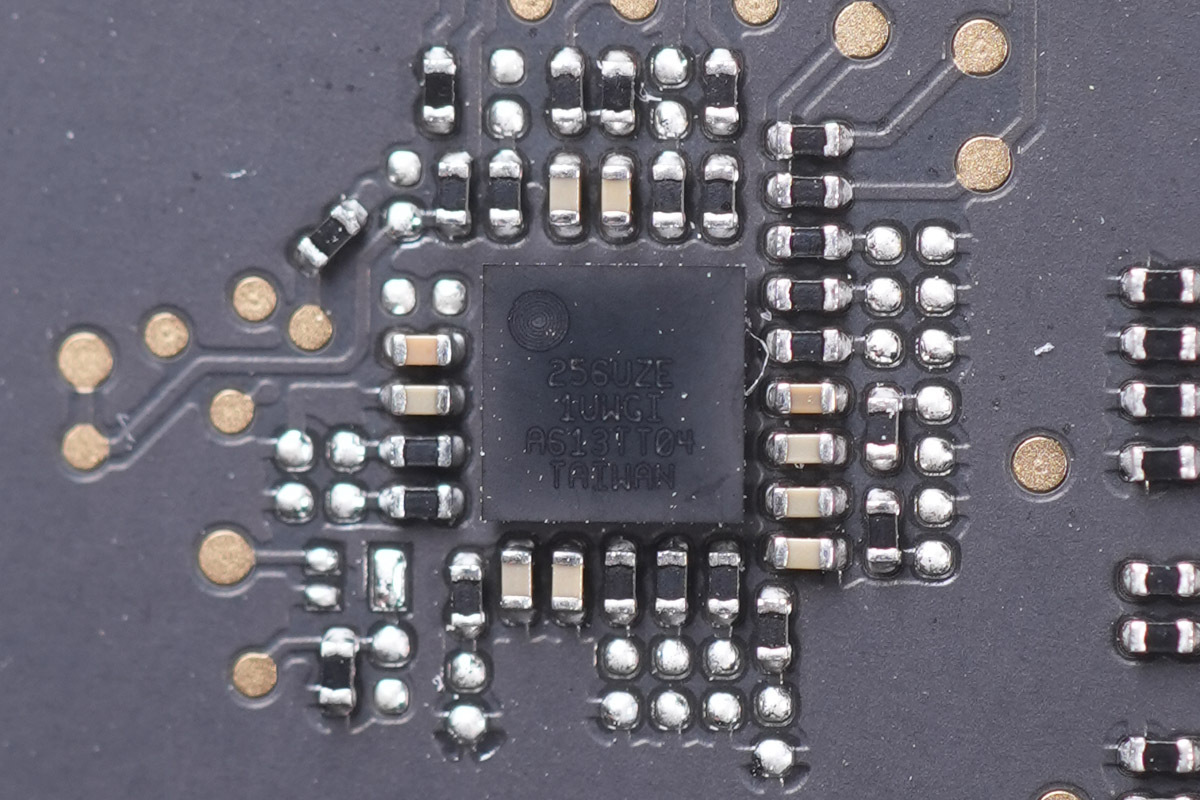
The FPGA is from LATTICE, marked 256UZE-1UWGI.
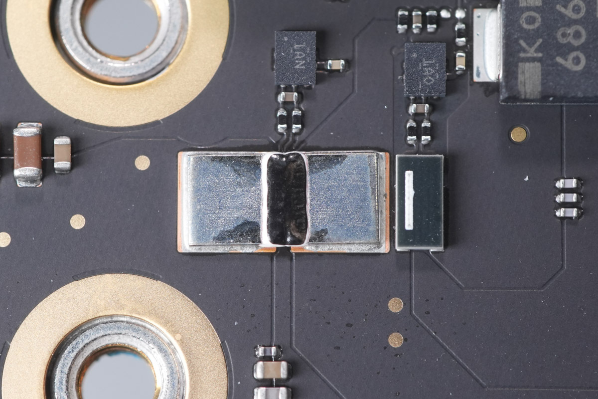
Two current-sense resistors are located at the power input end.
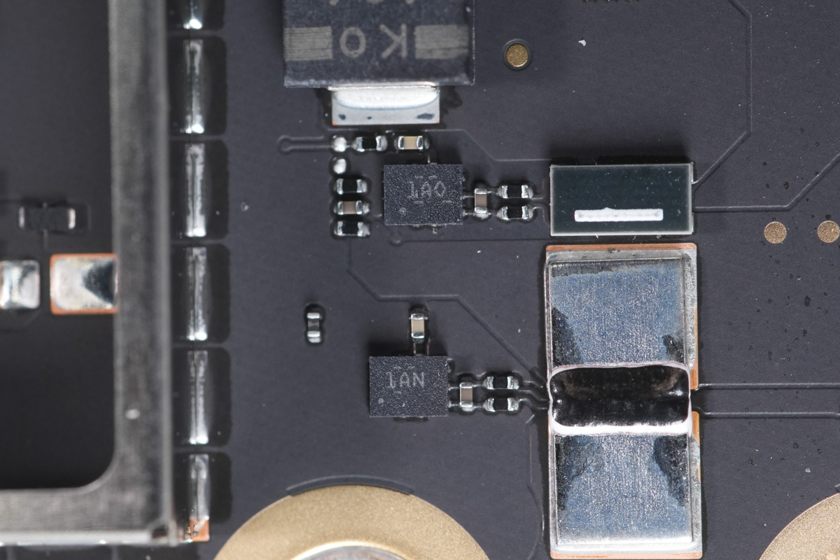
The current-sense amplifiers are from TI, marked 1AO and 1AN. Both are INA190 devices.
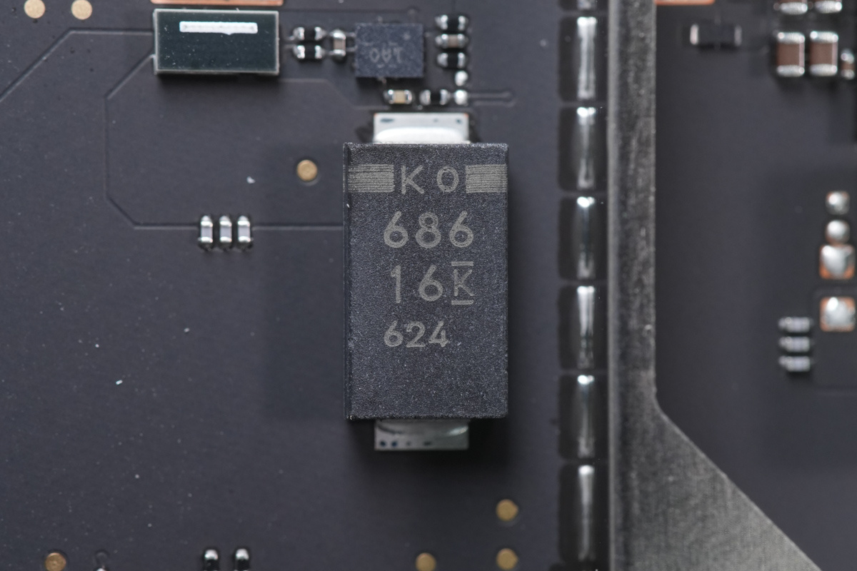
The filter cap is from KEMET, rated at 68 μF, 16 V.
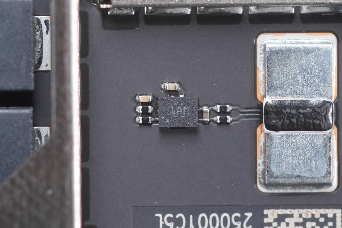
The current-sense amplifier is the TI INA190.
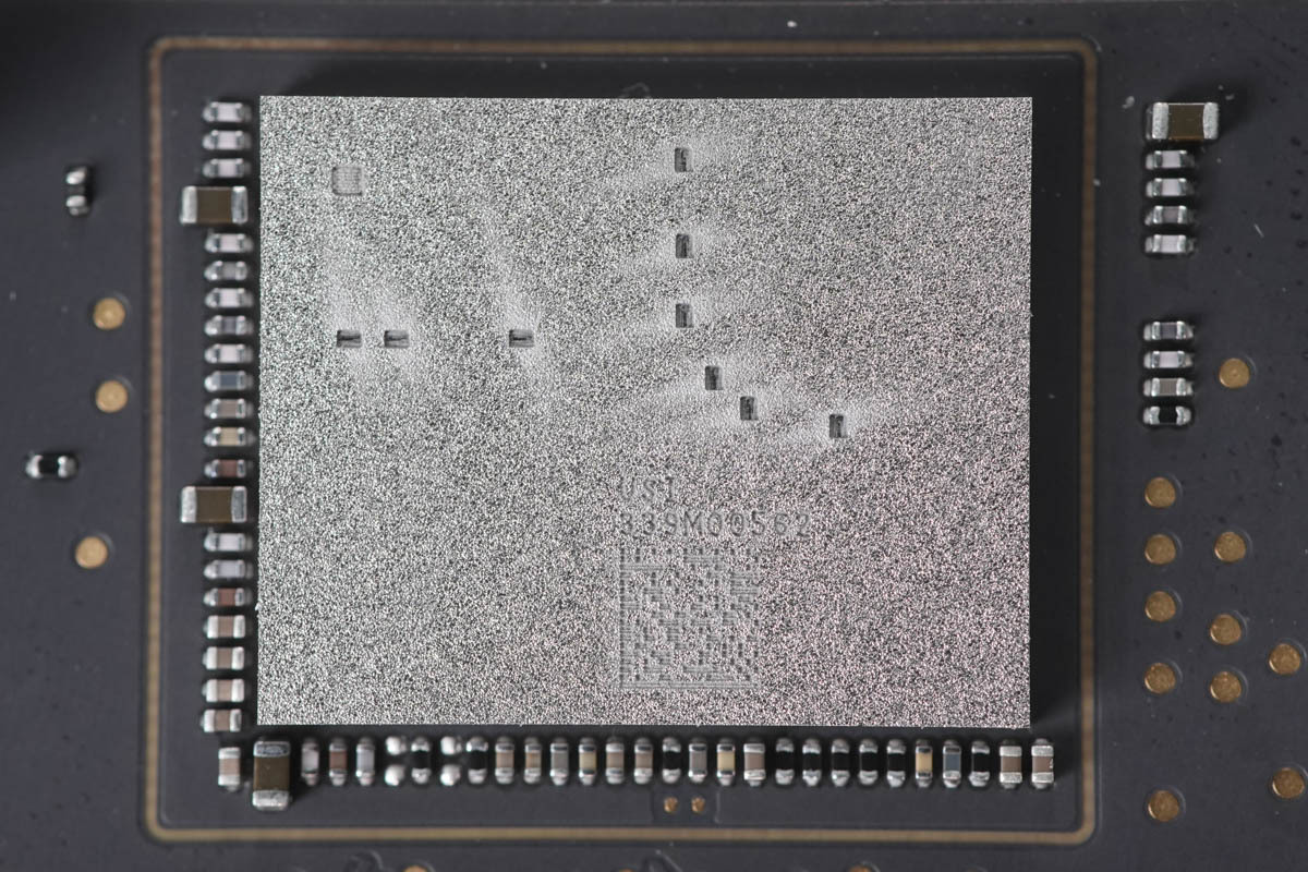
The wireless communication chip is marked USI 339M00562.
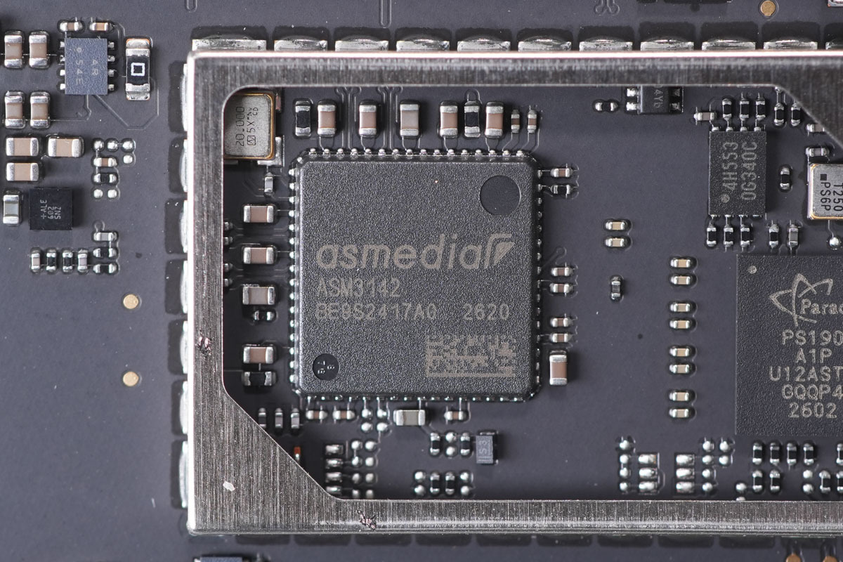
The USB conversion chip is from ASMedia, model ASM3142. It is a PCIe-to-USB 3.1 controller that converts PCIe Gen 3 x2 into two USB 3.1 Gen 2 ports supporting 10 Gbps data rates. It is housed in a QFN-64 package.
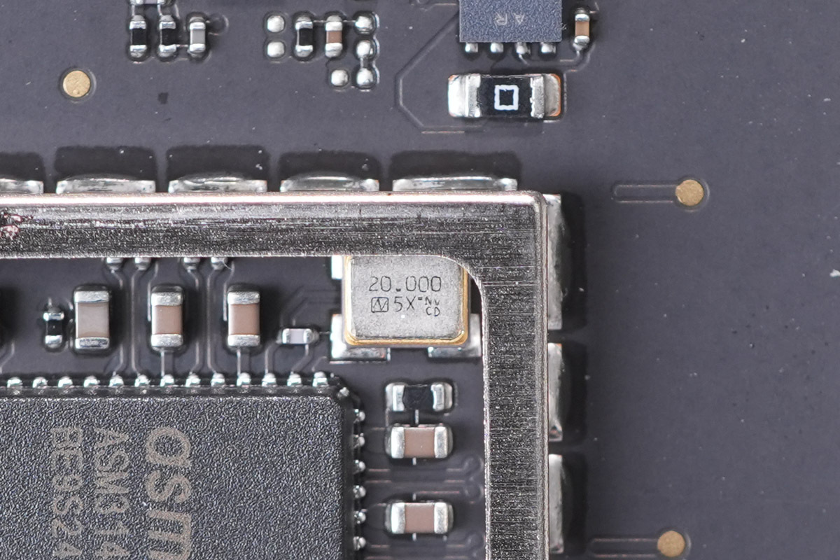
The 20.000 MHz clock crystal.
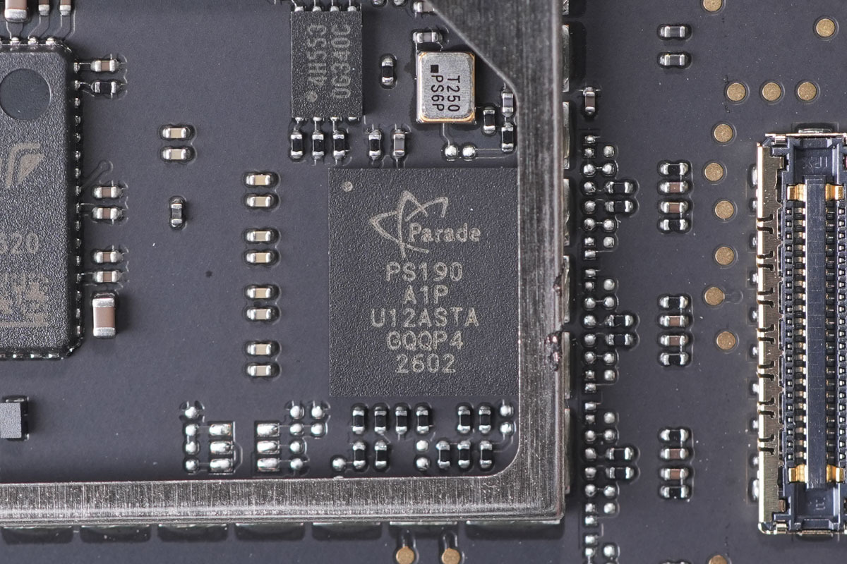
The video conversion chip is from Parade, model PS190, and converts DisplayPort (DP) signals to HDMI output.
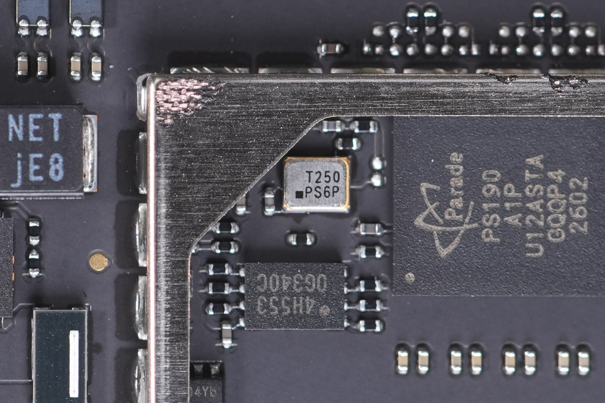
The external clock crystal.
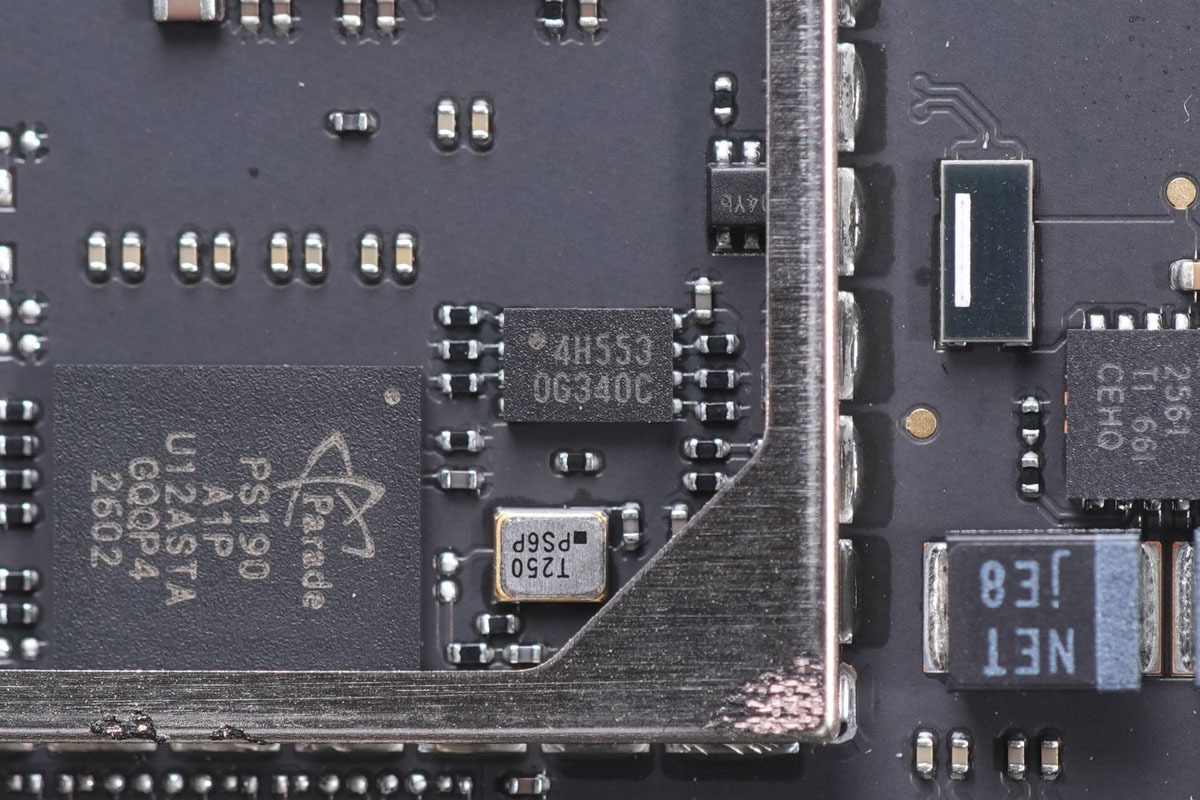
The memory is from Winbond, marked 4H, model W25X40CLUXIG, with a capacity of 512 KB. It supports an operating voltage of 2.3–3.6 V and is housed in an 8-pad USON package.
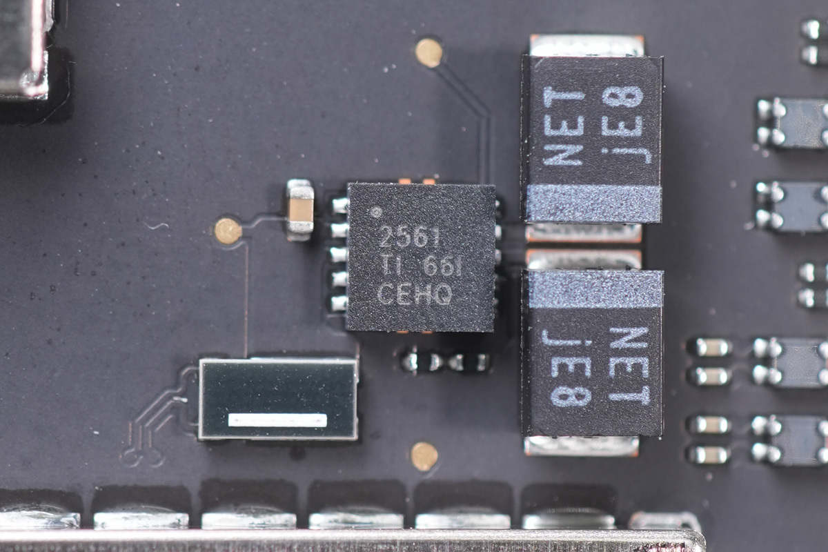
The USB power switch is from TI, model TPS2561. It is a dual-channel power switch with an adjustable current limit of 0.25–2.8 A, supports an operating voltage range of 2.5–6.5 V, and is housed in a VSON-10 package.
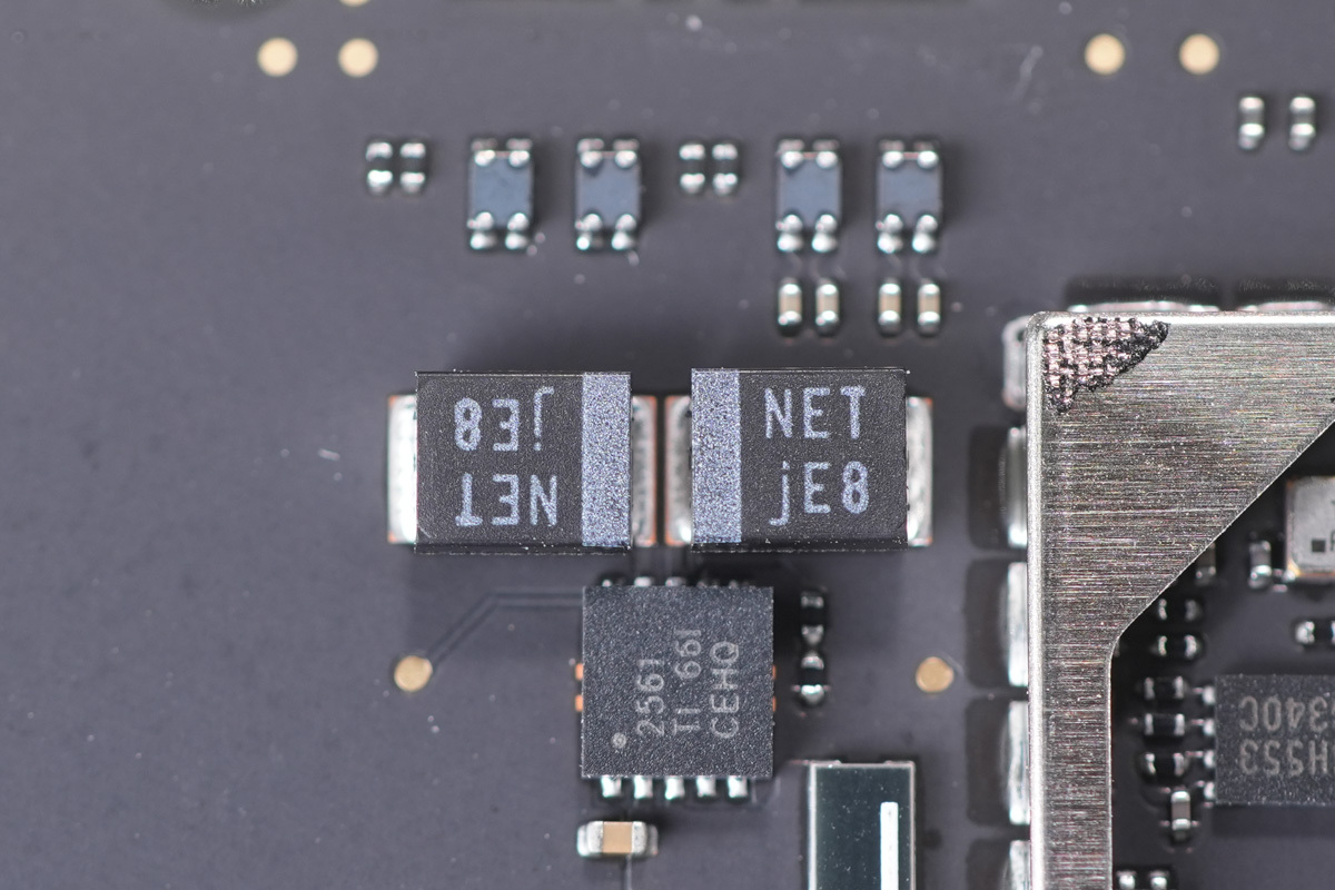
The filter cap is rated at 150 μF, 6.3 V.
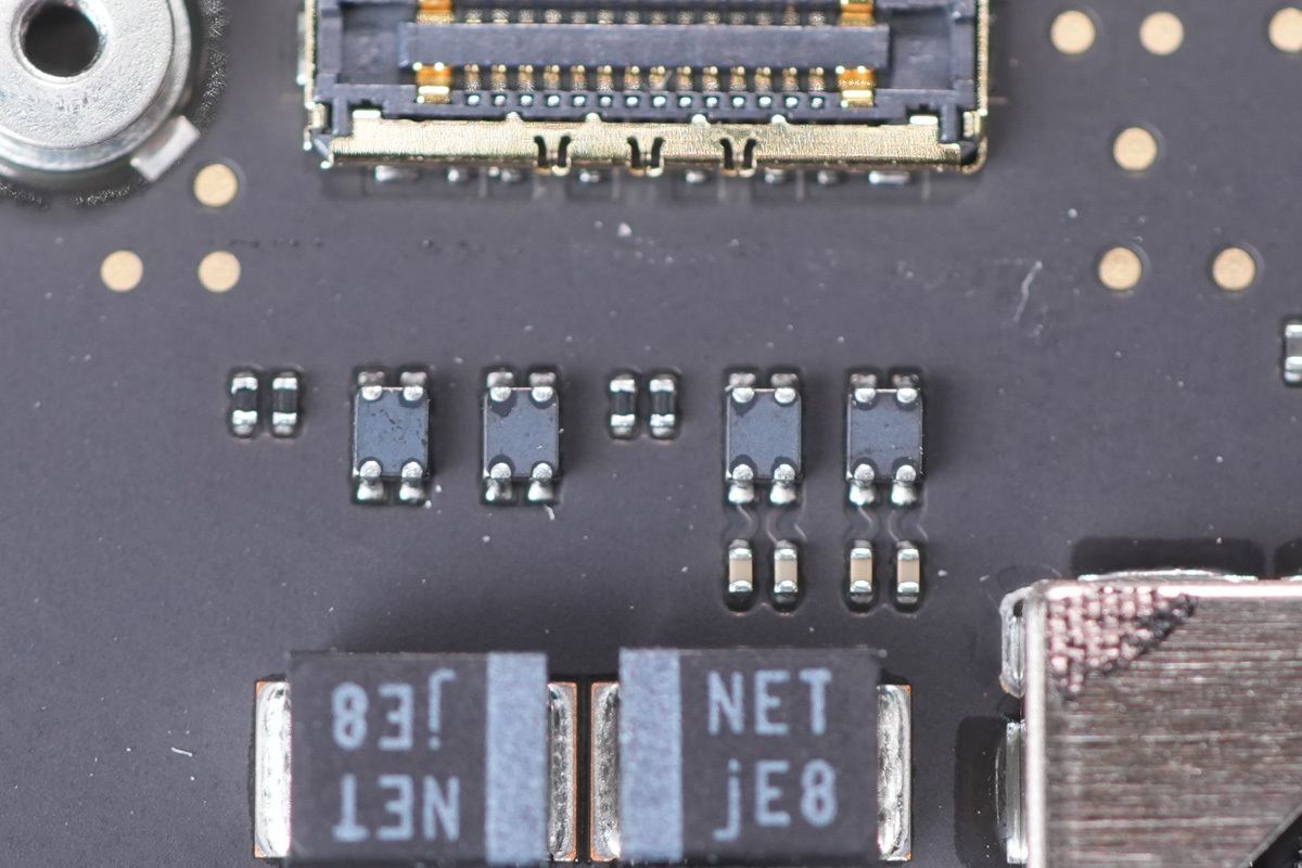
The HDMI port is equipped with a filter inductor.
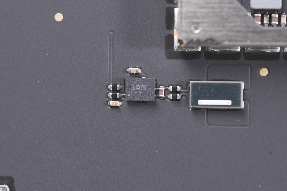
The current-sense amplifier is the TI INA190.
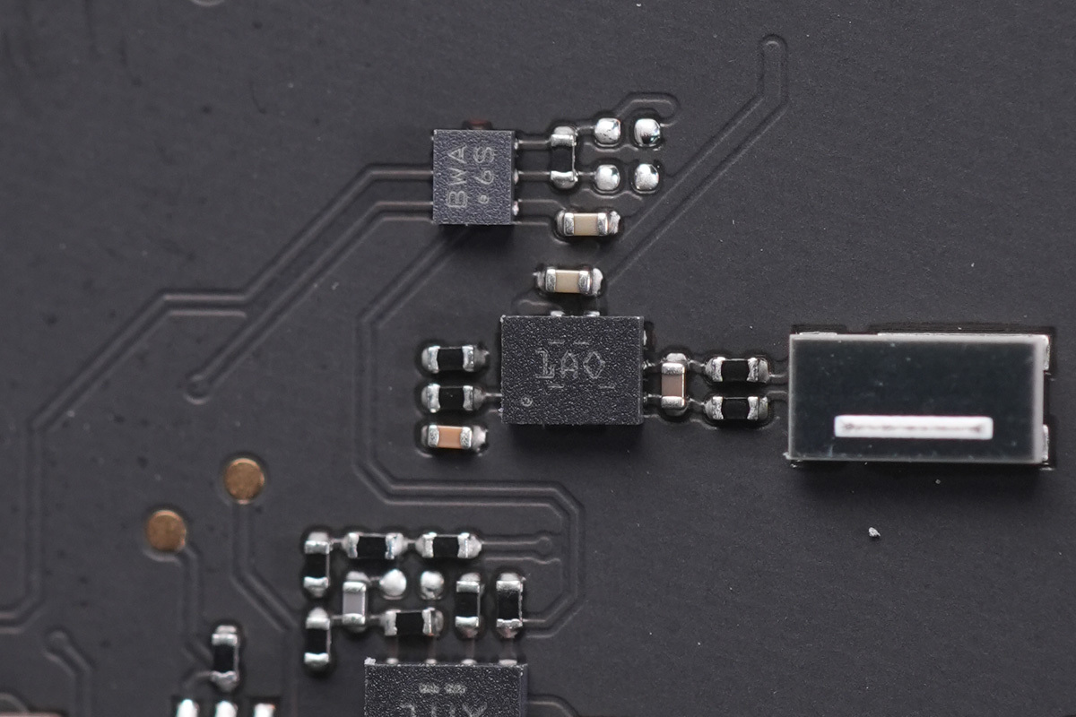
The current-sense amplifier is the TI INA190.
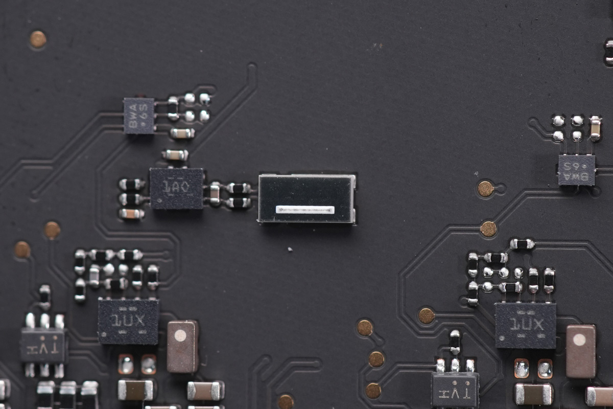
The corresponding current-sense resistor.
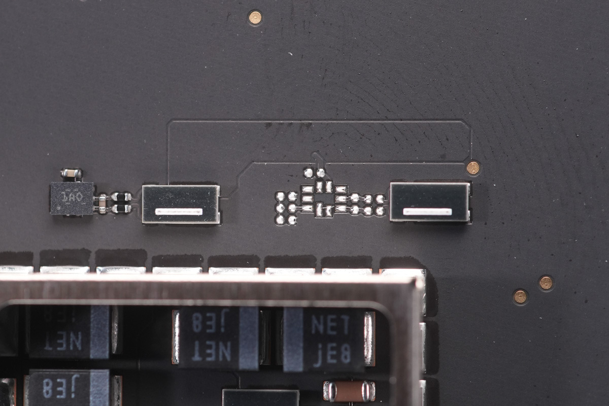
The two current-sense resistors.
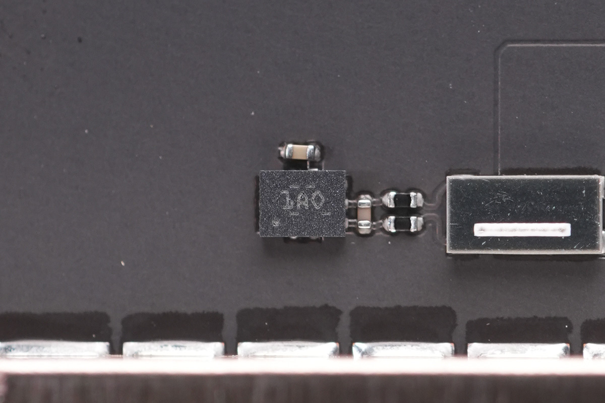
The current-sense amplifier is the TI INA190.
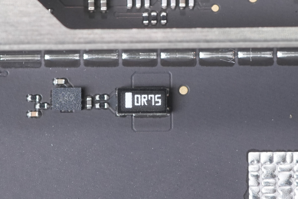
The current-sense resistor is marked 0R75.
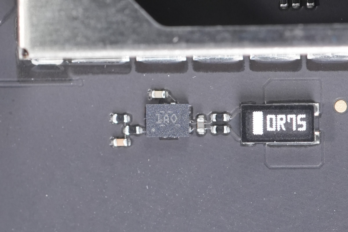
The current-sense amplifier is the TI INA190.

The current-sense amplifier is the TI INA190.
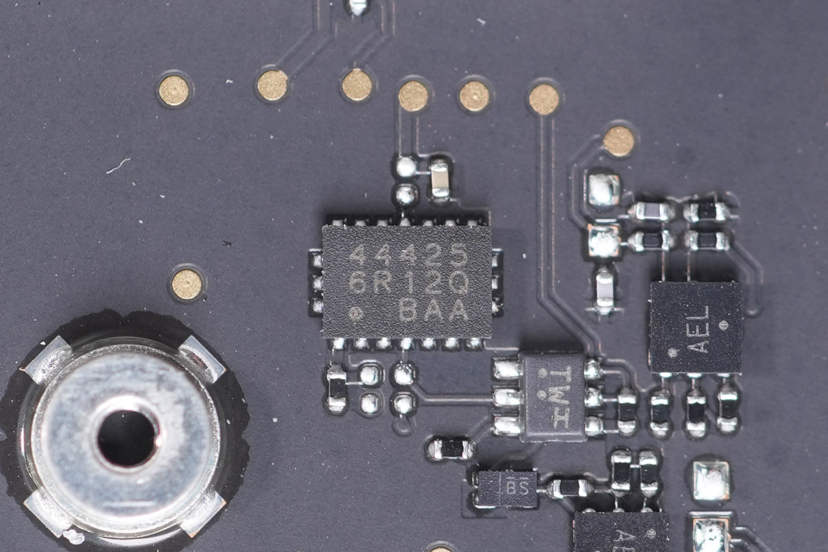
The chip marked 44425.
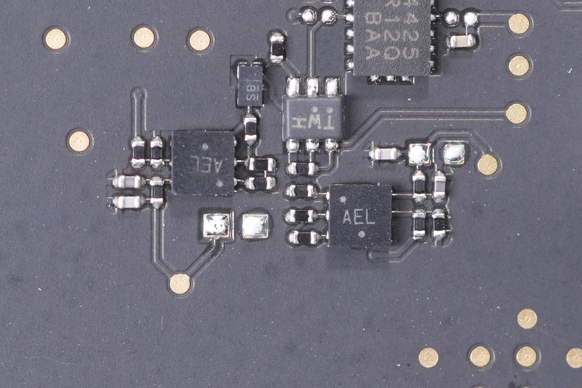
The chip marked AEL.
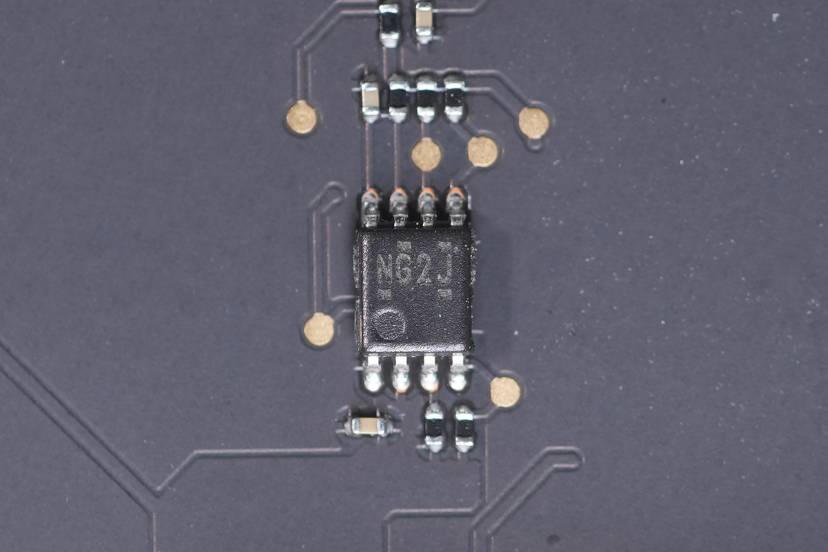
The level shifter is from TI, marked NG2J, model LSF0102. It is a dual-channel, bidirectional, multi-voltage level translator for open-drain and push-pull applications, housed in a VSSOP-8 package.
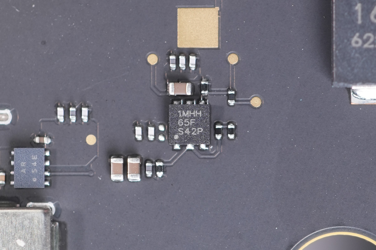
The voltage regulator is from TI, marked 1MHH, model TLV75801P. It is a high-precision adjustable linear regulator supporting an input voltage of 1.5–6 V and an output voltage of 0.55–5.5 V, with an output current of 500 mA. It is housed in a WSON-6 package.
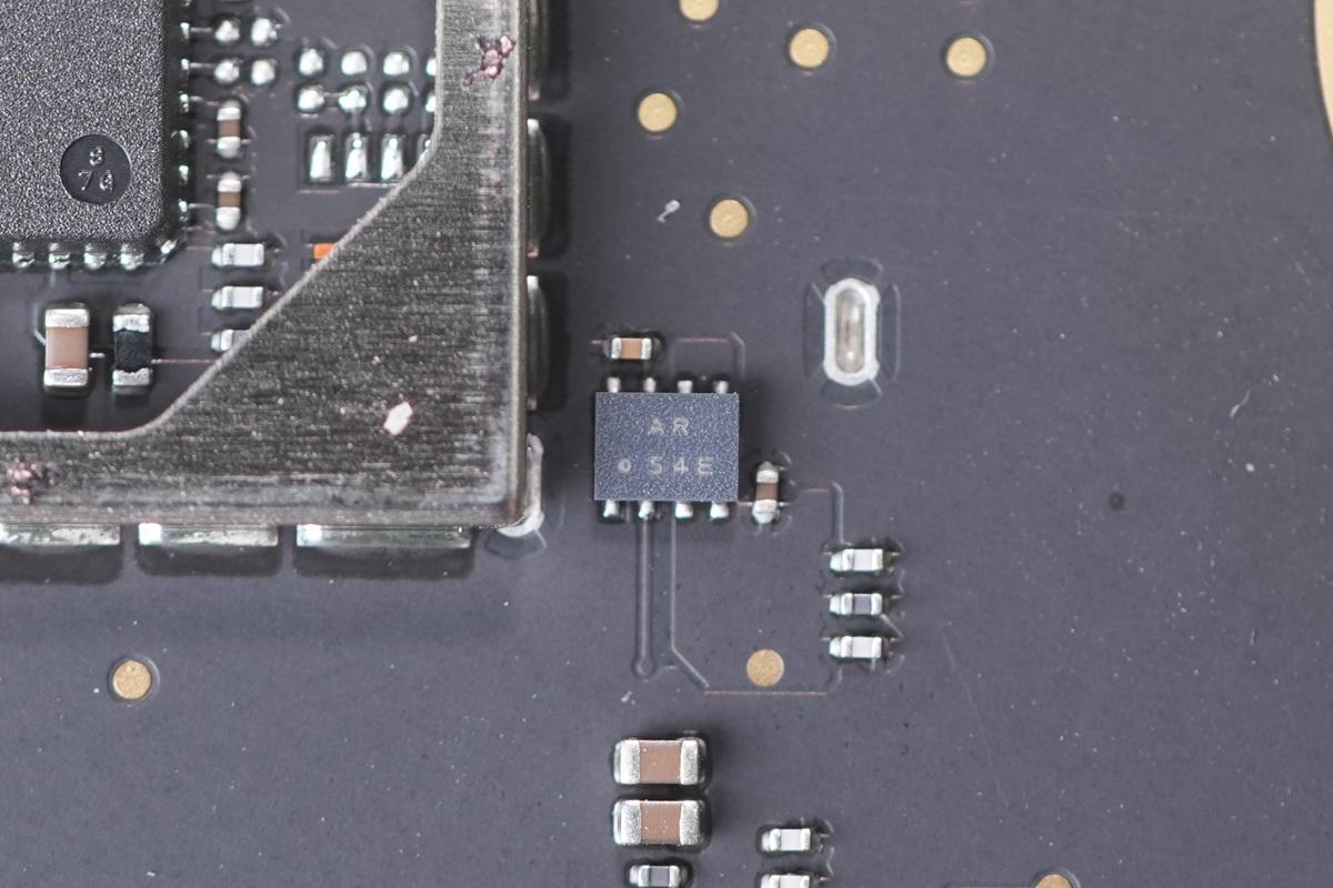
The chip marked AR.
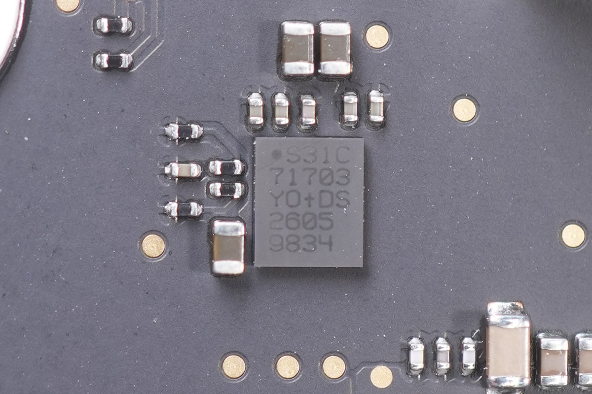
The chip marked S31C.
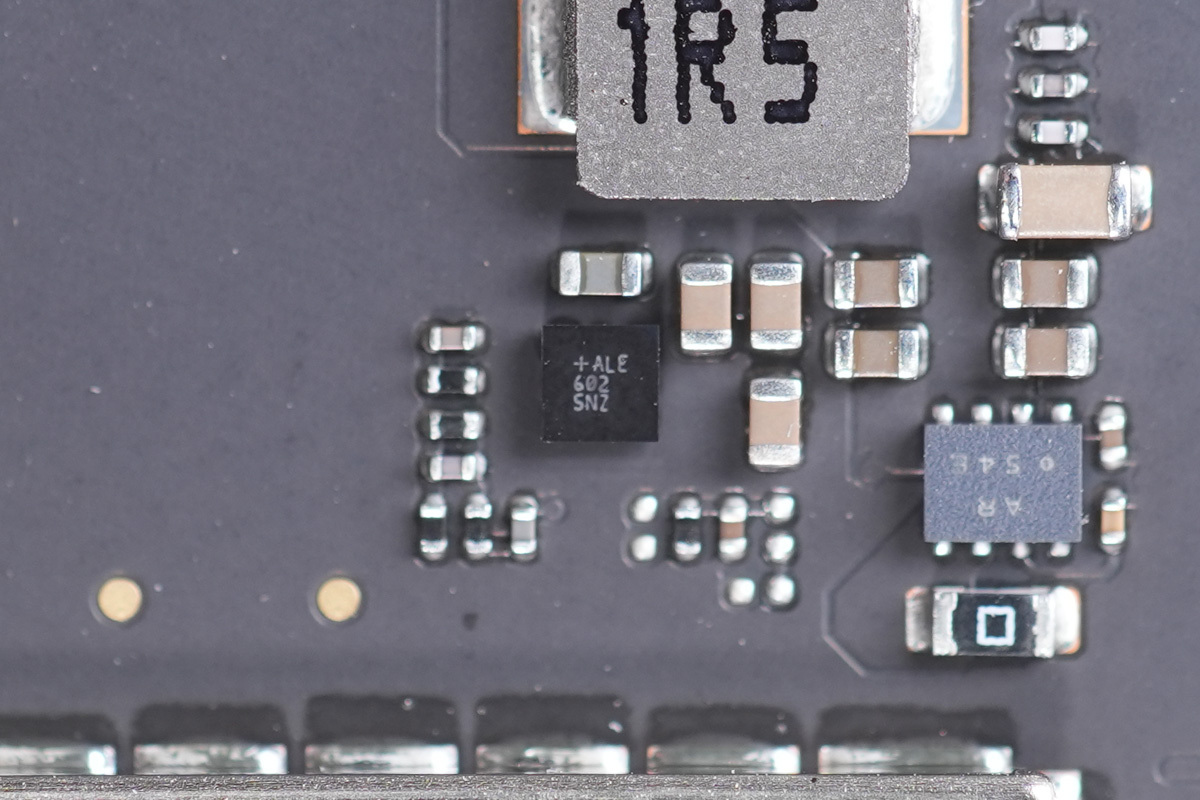
The chip marked ALE.
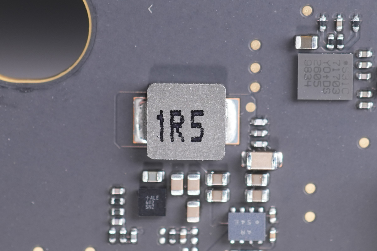
The 1.5 μH alloy inductor.
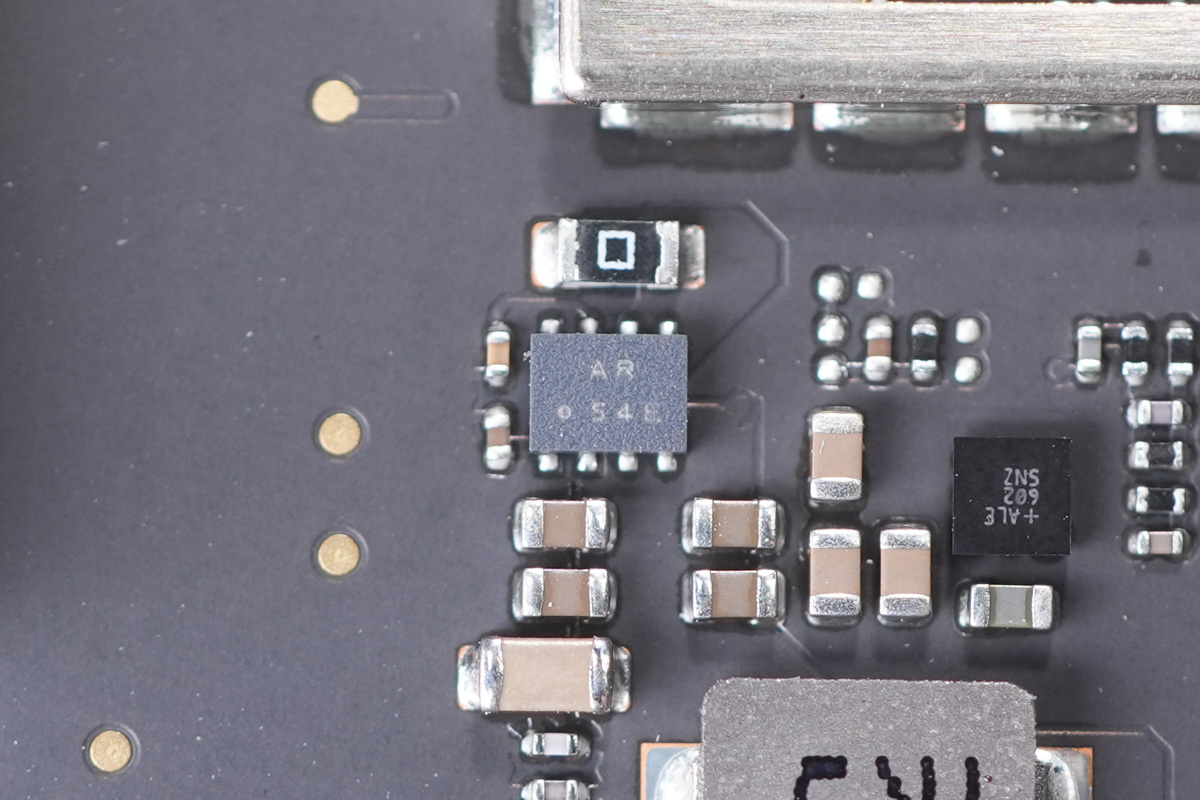
The chip marked AR.
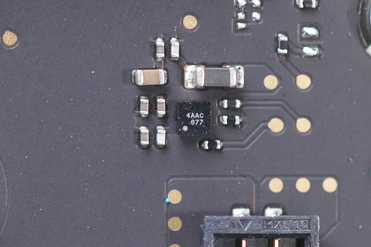
The chip marked 4AAC.
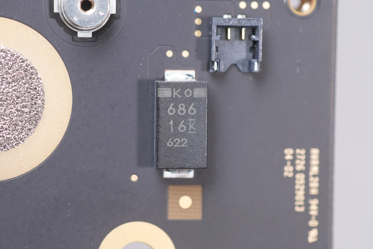
The filter cap is from KEMET, rated at 68 μF, 16 V.
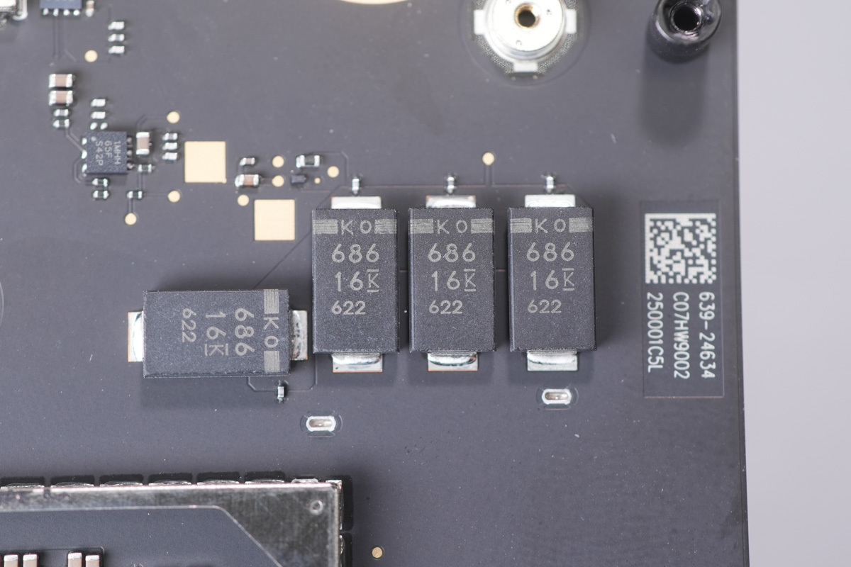
The filter caps are from KEMET, rated at 68 μF, 16 V.
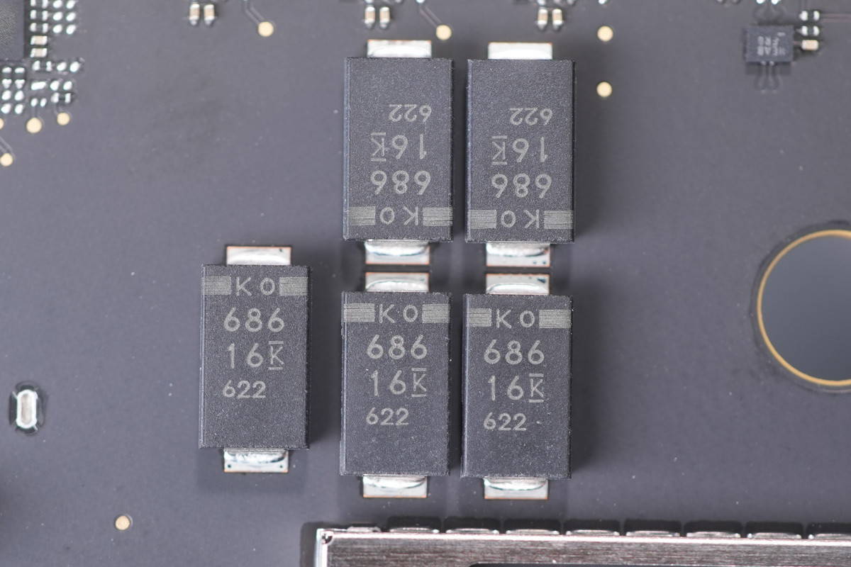
The filter caps are from KEMET, rated at 68 μF, 16 V.
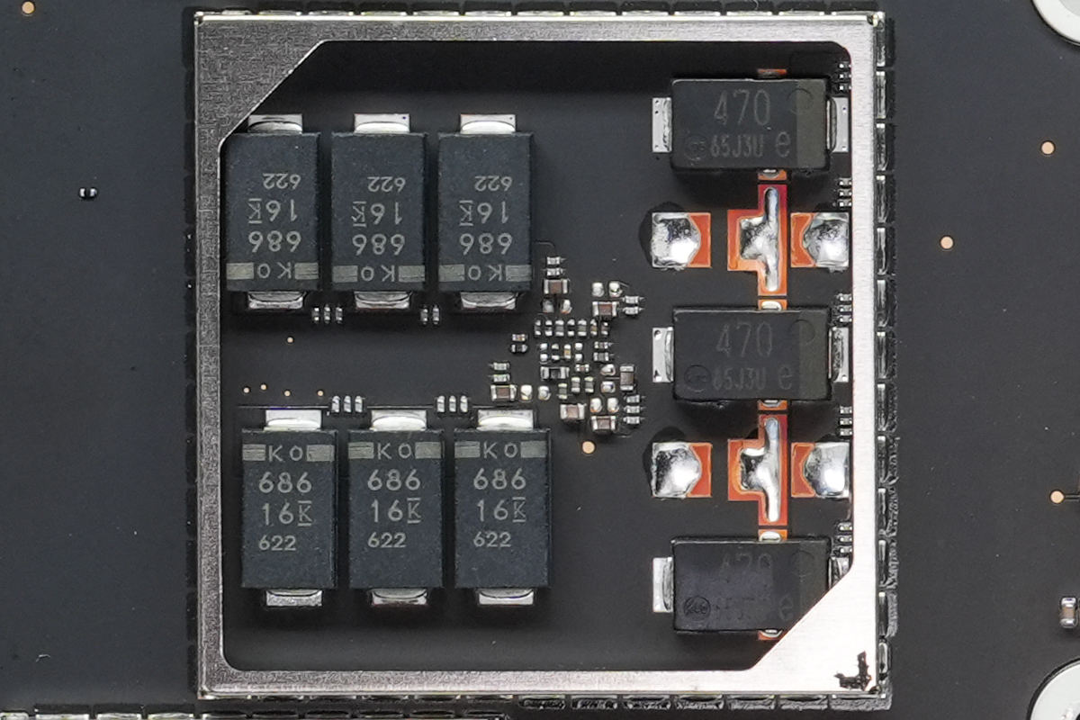
The left of the shielding can houses six 68 μF, 16 V filter caps, while the right side contains three 470 μF, 2.5 V filter caps.
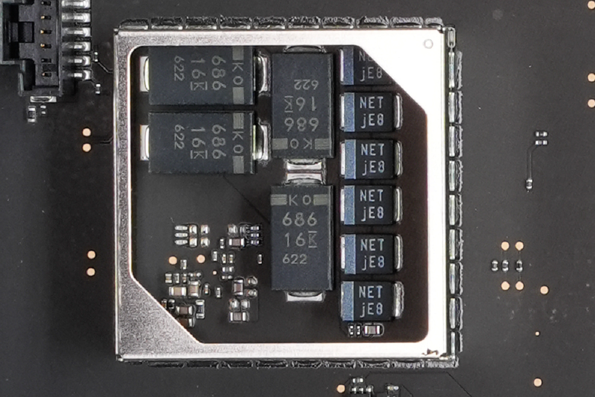
The left of the shielding can houses four 68 μF, 16 V filter caps, while the right side contains six 150 μF, 6.3 V filter caps.
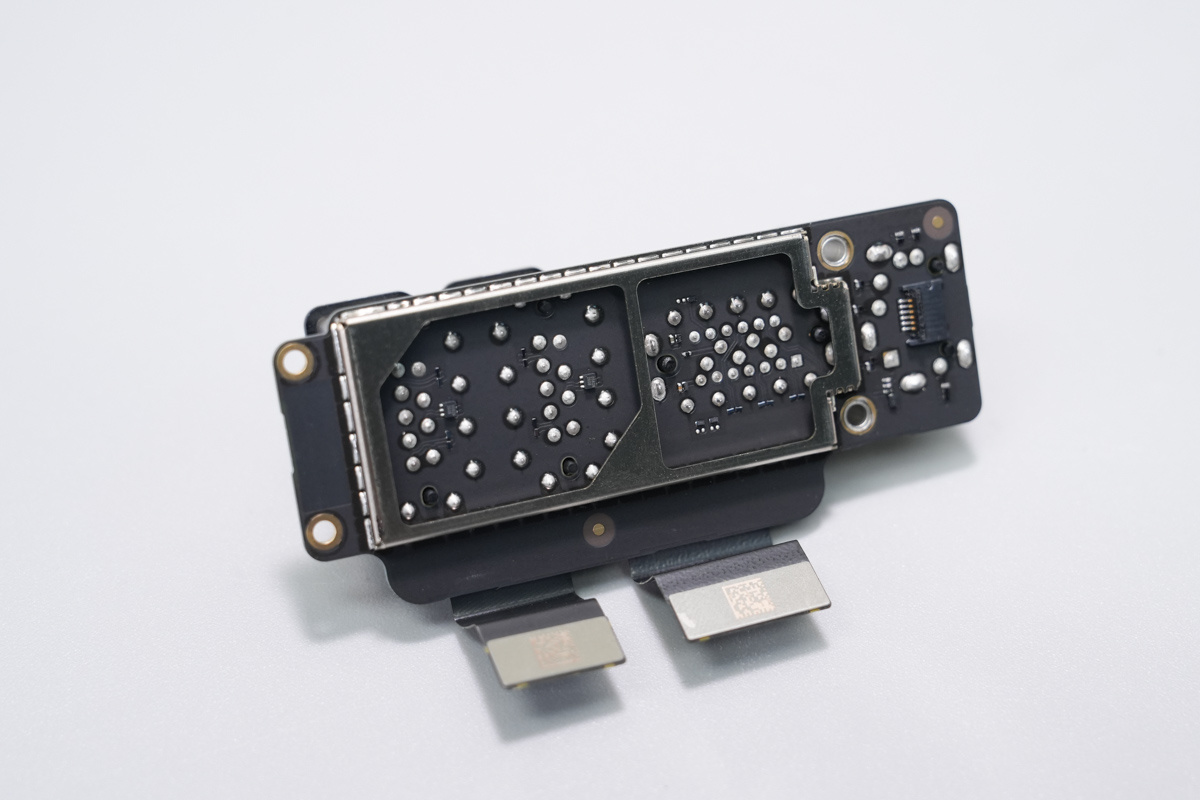
Remove the shielding can from the back of the interface PCB.
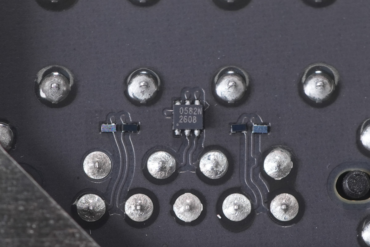
The USB-A data lines are equipped with ESD protection diodes.
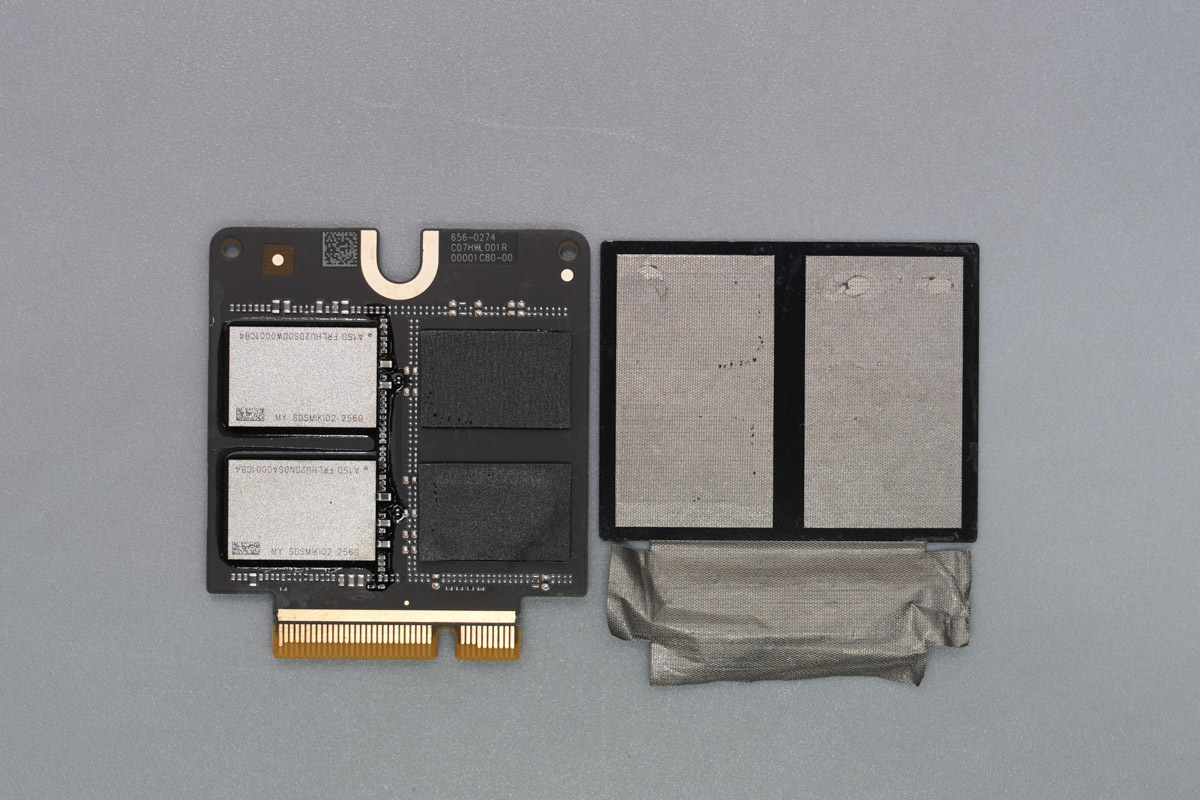
Conductive fabric is attached to the SSD PCB.
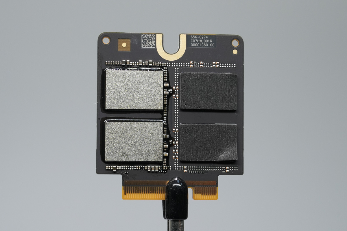
The front of the PCB features two flash memory chips.
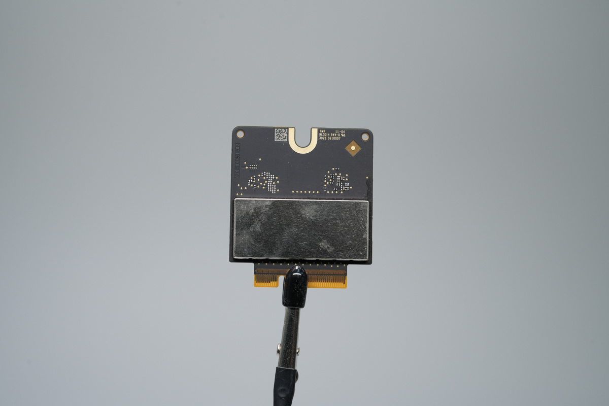
The back features a shielding can.
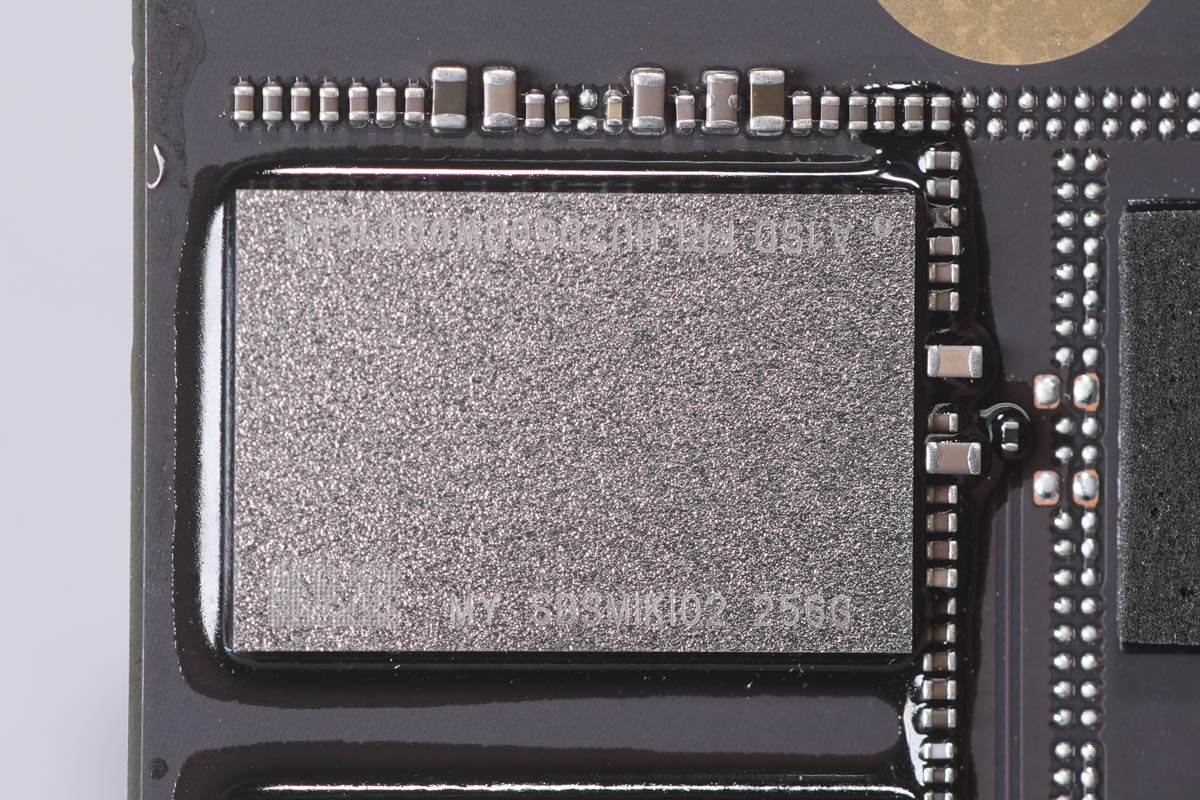
The flash memory chip is marked SDSMIKIO2 256G.
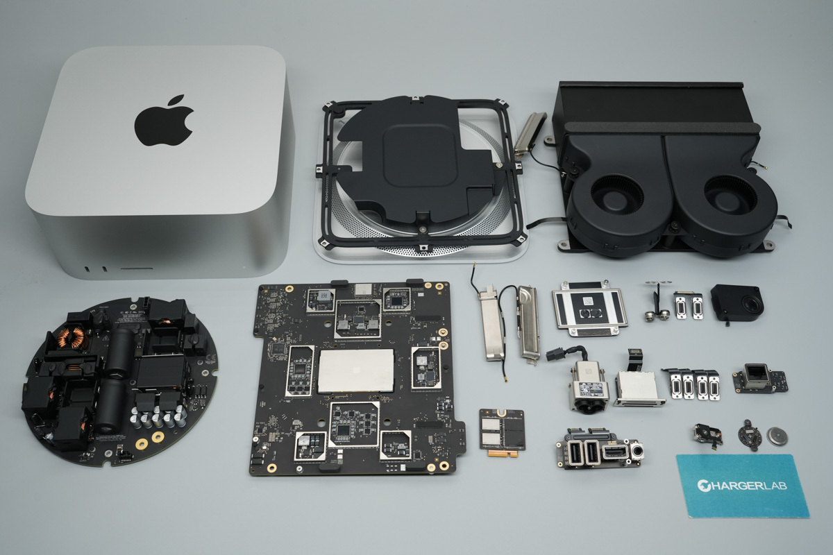
Well, those are all components of the Apple Mac Studio (M5 Max, A3545).
Summary of ChargerLAB
The Apple Mac Studio sports a sleek silver aluminum enclosure. Up front, you get two USB-C ports, an SD card slot, and a power indicator; around back, it packs four high-speed Thunderbolt 5 ports, two USB-A ports, 10Gb Ethernet, and an HDMI port. Powered internally via a standard cloverleaf AC cable, the chassis draws intake air from the perforated base and exhausts heat through the rear thermal mesh.
ChargerLAB's teardown shows a clean, dual-tier stacked interior: a power supply board sits at the bottom, while the main logic board rests above it. Mounted on top of the logic board is the M5 Max chip, cooled by a heavy-duty thermal module featuring dual centrifugal fans and a large copper/aluminum fin array.
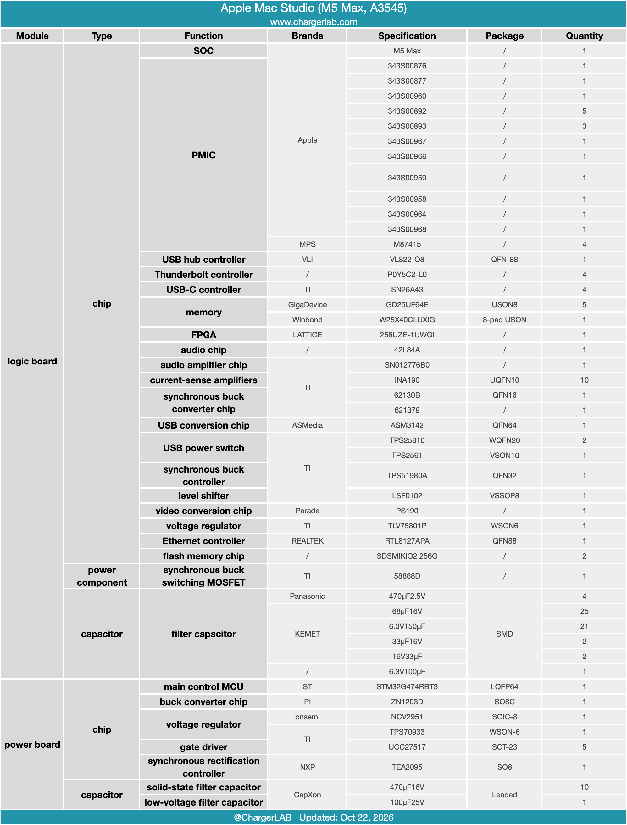
The power supply board runs on an Interleaved PFC + LLC + Synchronous Rectification architecture. Primary PFC and LLC timing are managed by an ST STM32G474RBT3 MCU driving MOSFETs via TI UCC27517 drivers. Synchronous rectification is handled by an NXP TEA2095 controller with CapXon solid caps on filtering duty. Controller auxiliary power is generated via a PI ZN1203D buck IC and an onsemi NCV2951 regulator.
The M5 Max SoC sits front and center on the logic board. Under the primary metal shield lies a bank of custom Apple and MPS power management ICs (PMICs), power inductors, and filter caps. Auxiliary controller logic includes a VLI VL822-Q8 USB hub chip, an ASMedia ASM3142 USB converter, a Parade PS190 display converter, and a REALTEK RTL8127APA Ethernet controller, with filtering provided by Panasonic and KEMET SMD caps.
Storage is handled via two SSD PCB slots with two 256GB flash memory chips, adding up to 512GB of storage. Every internal sub-assembly is thread-locked with precision screws, and all external I/O ports are bolted directly to the inner chassis frame before connecting to the logic board via ribbon cables secured with metal clamp plates—a masterclass in modular serviceability and Apple's signature industrial design.
Related Articles:
1. Teardown of the Apple Mac mini (M6, A3534)
2. Charging Review of iPhone 18 Pro Max
3. Teardown of Apple M4 Mac mini (A3238)
