

Introduction
Recently, ChargerLAB acquired a high-power outdoor programmable LED driver from Inventronics, engineered specifically for rigorous environments like street and area illumination.
The unit supports an ultra-wide AC input range of 90–305V, delivering exceptional conversion efficiency alongside an IP67 ingress protection rating.
As an intelligent LED driver, it offers versatile dimming options—including 1(0)–5V, 1(0)–10V, PWM, resistance, and timer-based scheduling. By integrating advanced GaN and SiC power semiconductors internally, this high-wattage supply achieves superior efficiency and reliability within a streamlined enclosure.
ChargerLAB now presents a comprehensive teardown of this Inventronics programmable LED power supply to inspect its internal circuit design and component selection.
Product Appearance
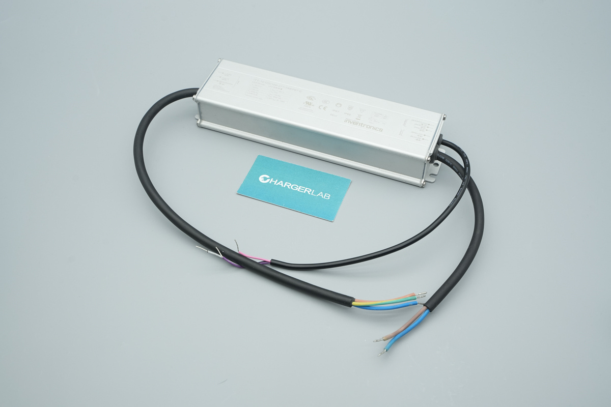
The Inventronics programmable LED control power supply features a silver extruded aluminum long strip-shaped sealed chassis, with input and output/control cables routed from both ends respectively.
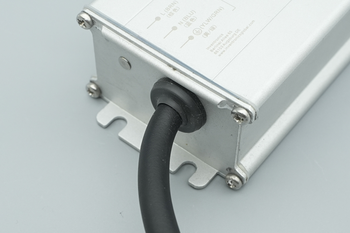
The base of the input cable is fitted with a thick black rubber sealing ring, tightly integrated with the aluminum alloy casing to ensure outstanding waterproof and dustproof performance.
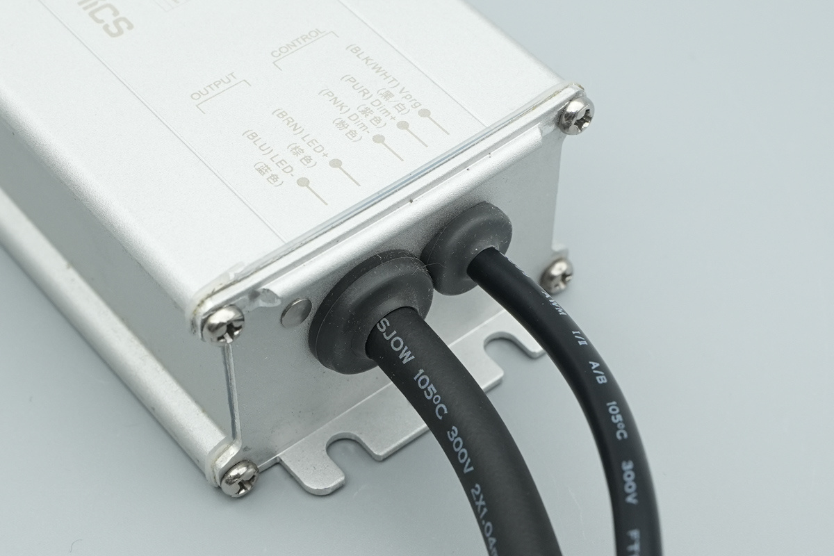
The other side houses the output and dimming control cables, which are similarly sealed and protected using dual rubber rings.
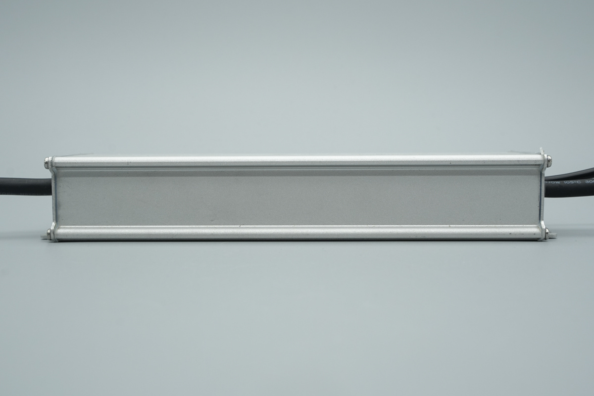
The casing is manufactured using an extrusion process with reinforcing grooves on both sides of the body.
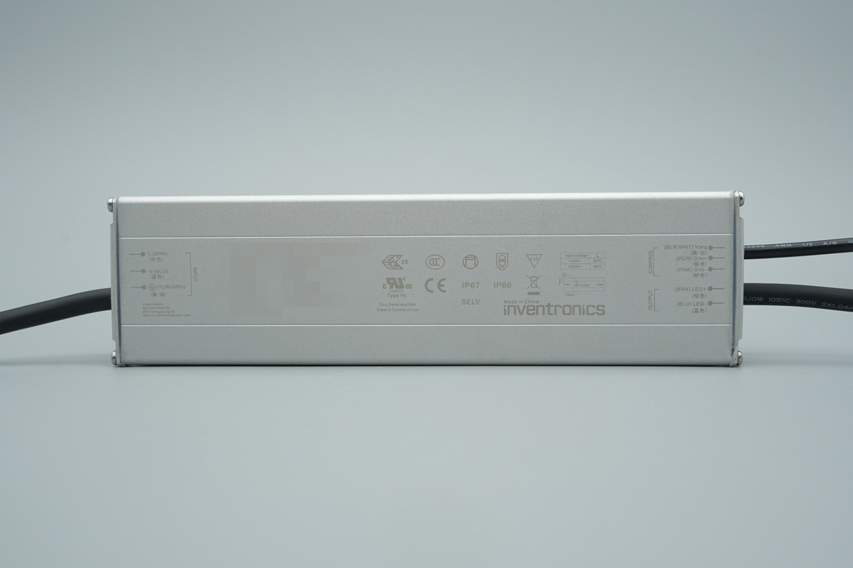
The surface of the casing is laser-engraved with detailed product parameters and certification marks like ENEC, UL, CCC, and CE.
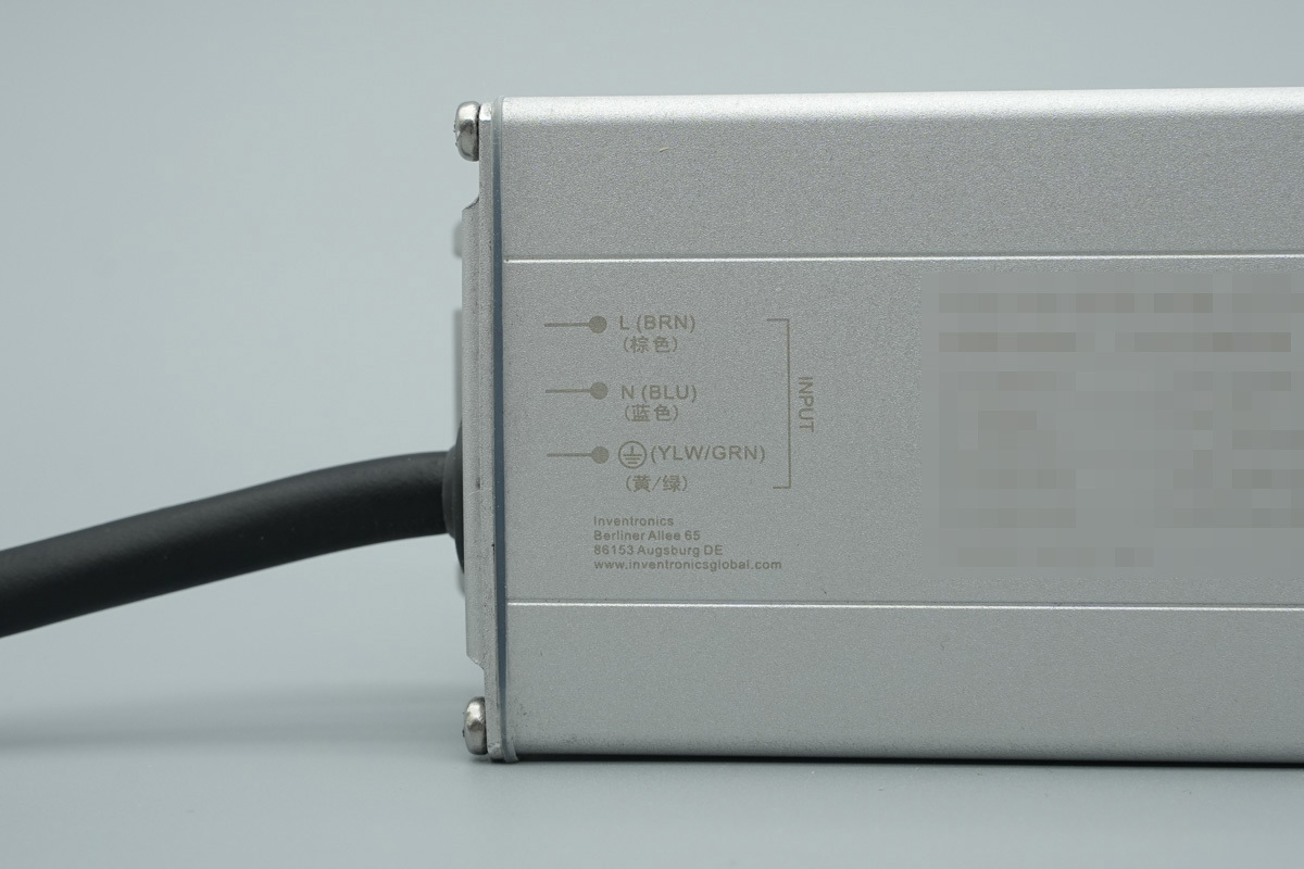
The input end of the nameplate outlines the pinout definitions: L (BRN), N (BLU), and ground.
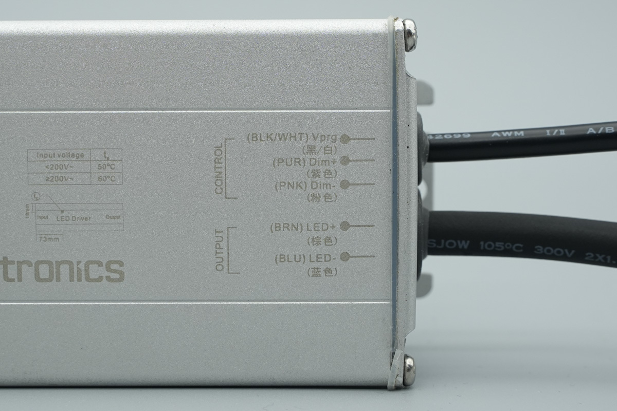
The output end displays the wiring definitions for LED+, LED-, and the control lines.
Physical Specifications
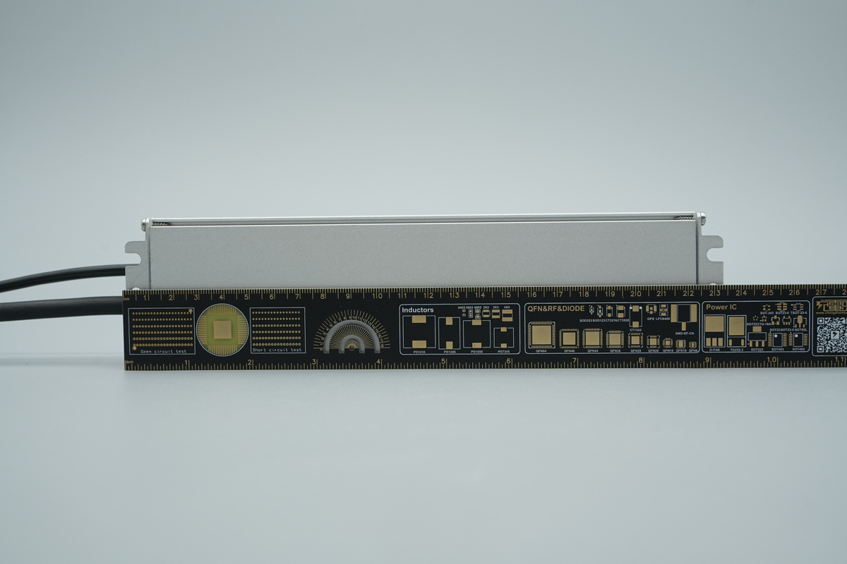
The length of the power supply is about 23.3cm (9.173 inches).

The width of the power supply is about 60.51mm (2.382 inches).
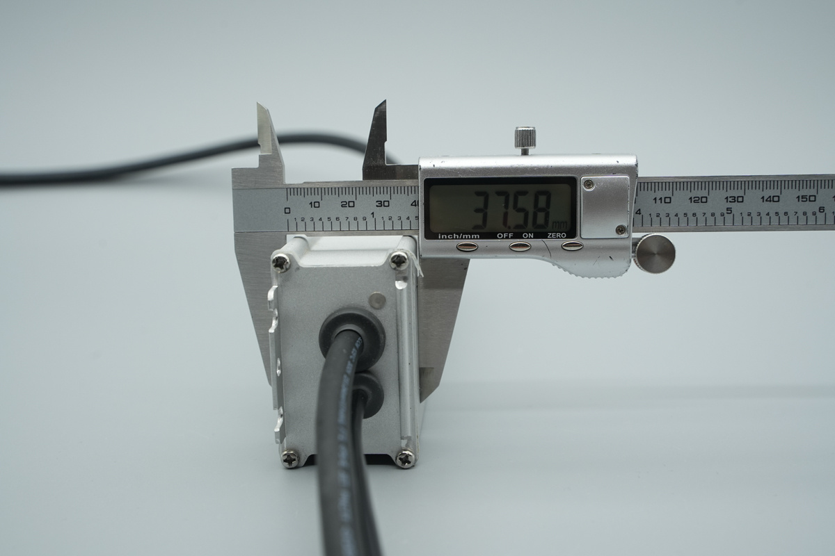
The thickness of the power supply is about 37.58mm (1.480 inches).
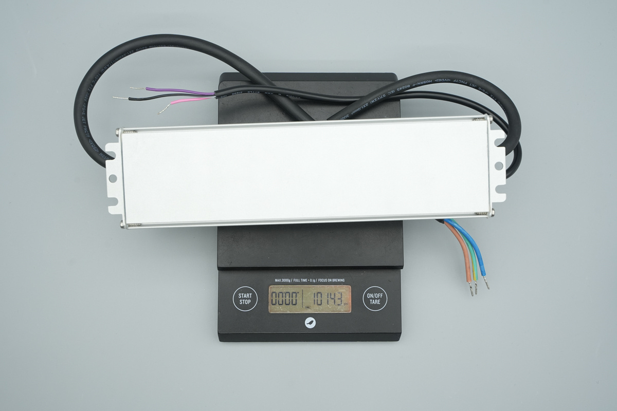
The weight is about 1014.3g (35.778 oz).
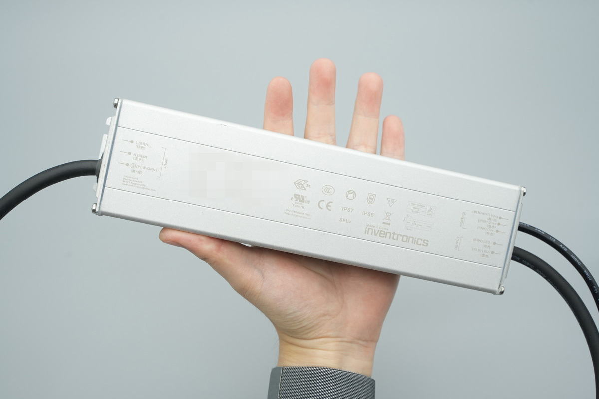
That's how big it is in the hand.
Internal Construction
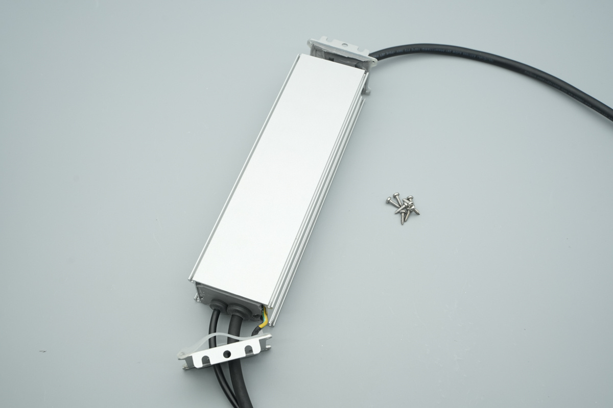
First, unscrew all the Phillips fixing screws on the metal cover plates at both ends of the body.
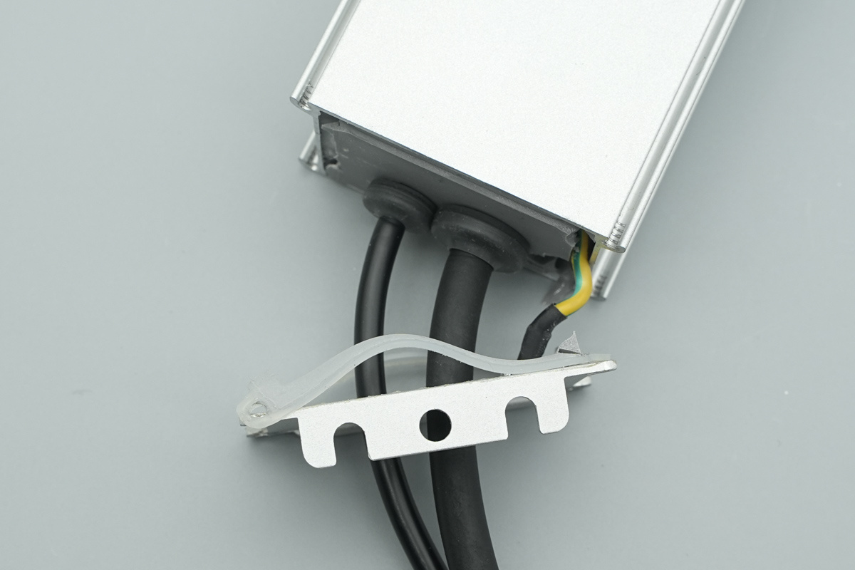
After removing the cover plate on one side, it can be seen that the interior is completely filled with a large amount of gray thermal potting compound, which is a necessary process to achieve IP67 waterproofing and thermal conductivity for high-power power supplies.

After cutting open the product casing, the internal PCBA module is exposed, showing that the entirety is covered with gray potting compound.
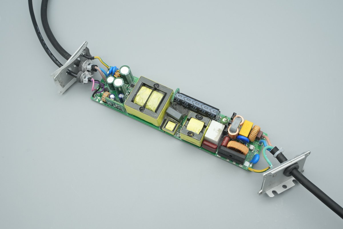
Cleaning away the thermal potting compound on the surface and around the perimeter reveals the component layout of the PCBA.
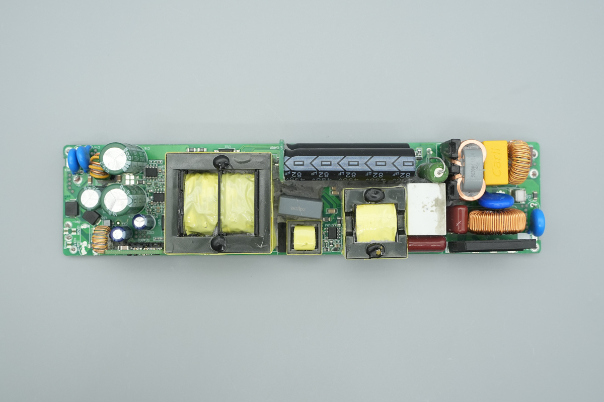
After removing the wires, it can be seen that this mainboard features a long strip-shaped design with high space utilization. From right to left, components such as the EMI filtering circuit, high-voltage filter caps, transformer, PFC choke, low-voltage filter caps, and LED dimming PCB are arranged in sequence.
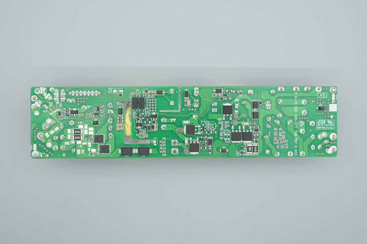
On the back, an obvious safety isolation gap can be seen between the primary and secondary sides, which are bridged via optocouplers and SMD Y-caps. The PFC diode, PFC MOSFET, primary MOSFET, SMD Y-caps, optocouplers, and synchronous rectifier MOSFETs are distributed in sequence. Overall, it can be seen that this Inventronics programmable LED control power supply adopts a PFC + LLC power architecture design.
Input EMI Filtering And PFC Circuit Analysis
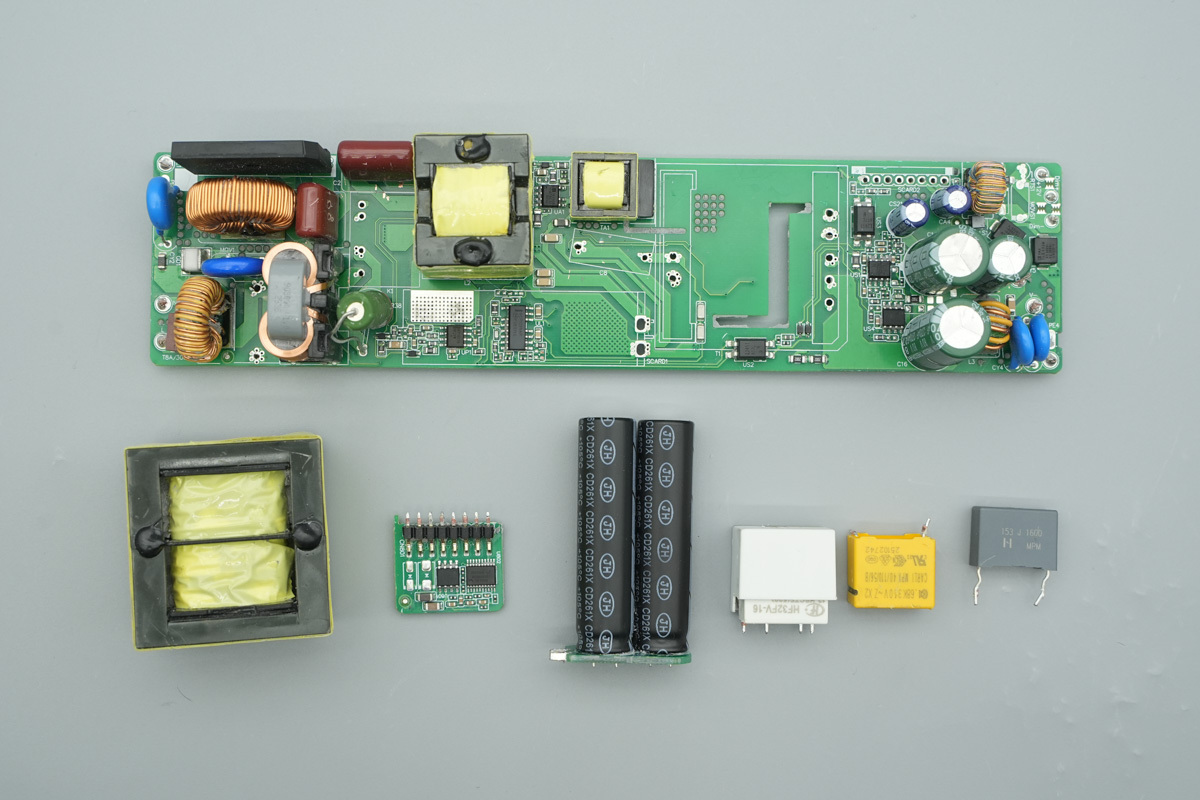
Continue by removing some components and the LED dimming PCB.
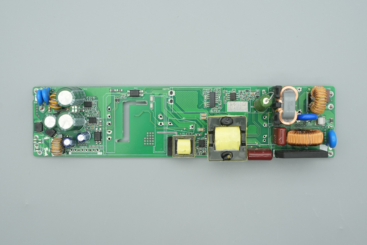
After removing some components, the PFC controller, LLC controller, and other components can be seen.
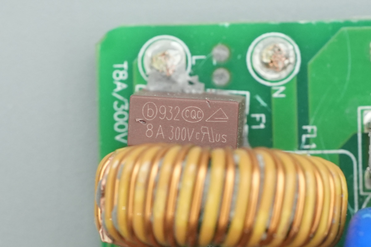
The input-end fuse is from Betterfuse, marked 932, spec 8A 300V, used for input OCP.
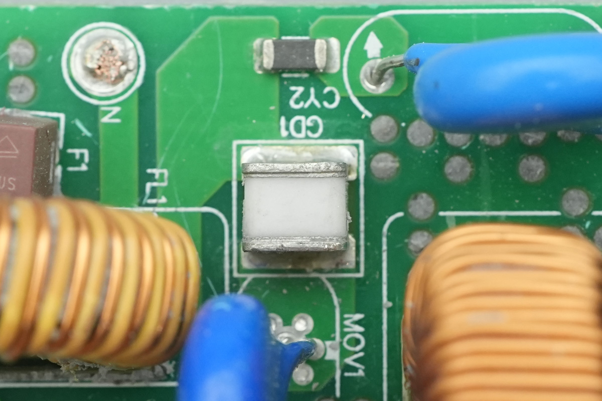
A ceramic gas discharge tube, used to absorb high-voltage lightning surges.
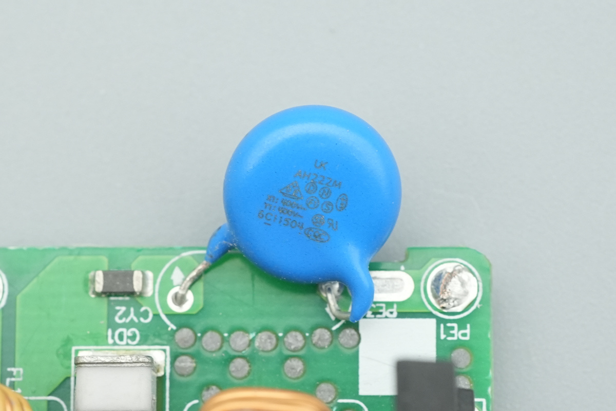
The blue Y-cap is from WTC, model AH222M.
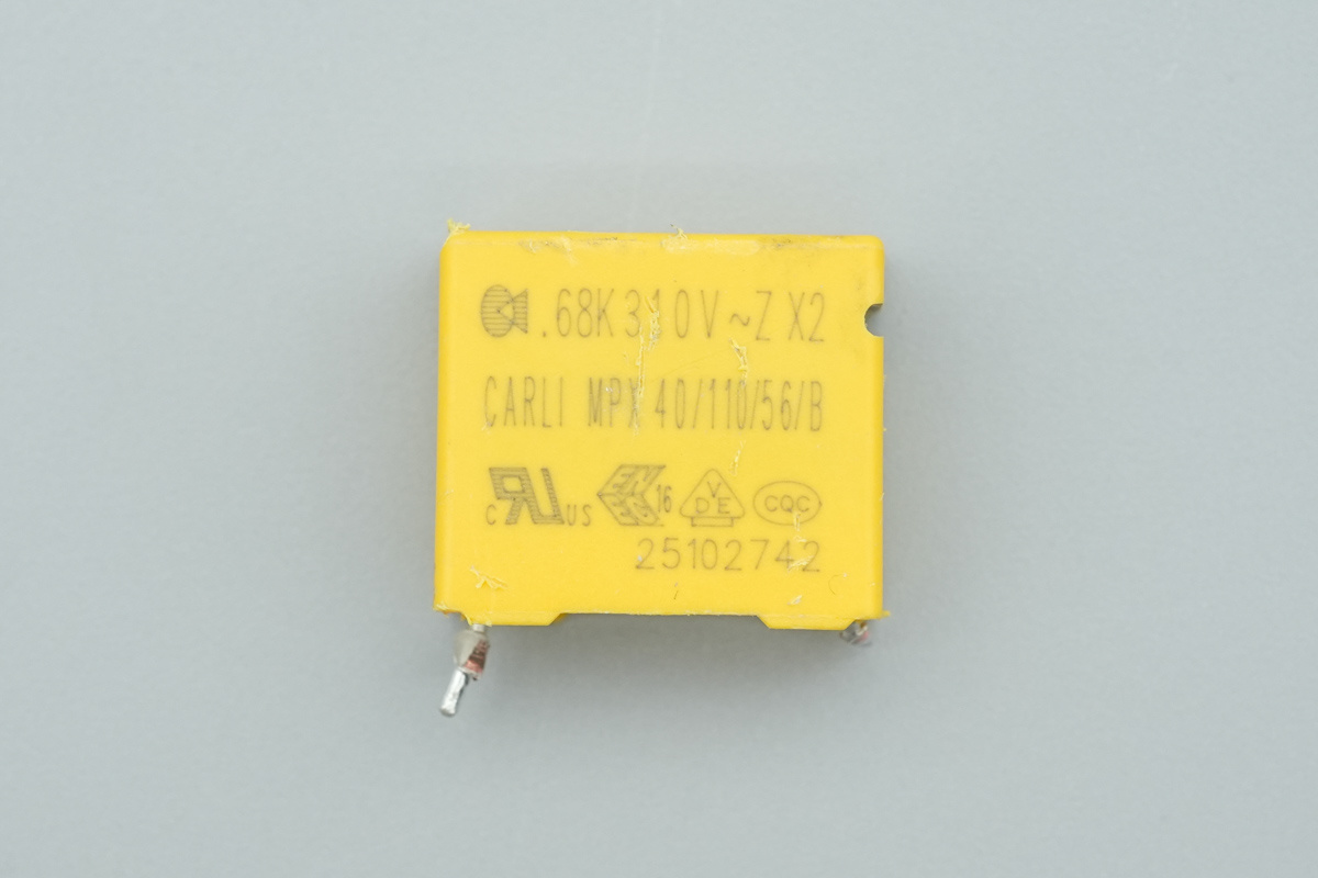
The safety X2 cap is from CARLI, spec 0.68μF.
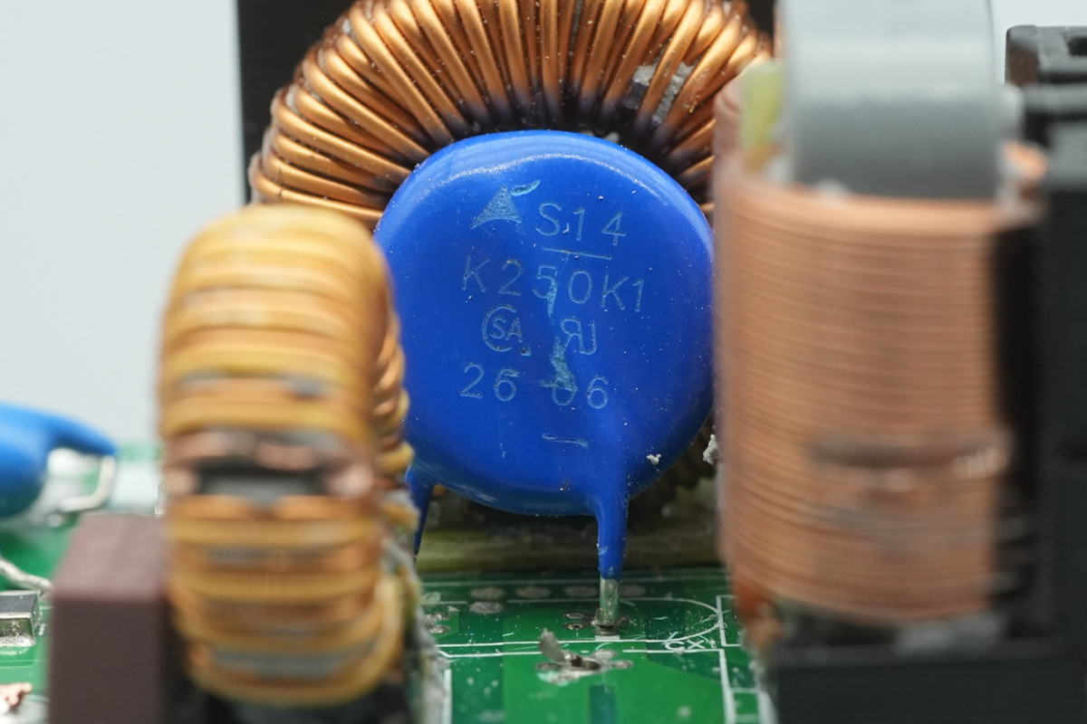
A varistor is from TDK, model S14 K250K1.
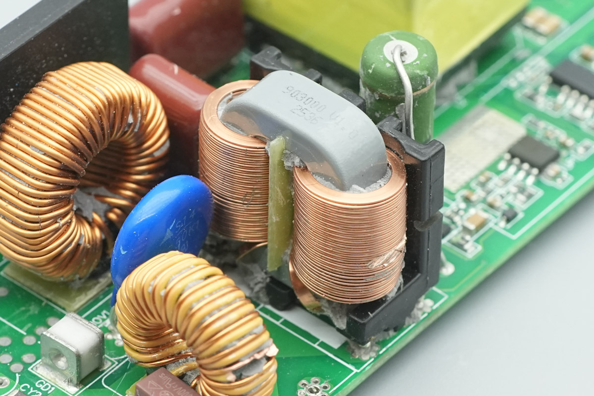
The common-mode choke is wound with flat copper wire.
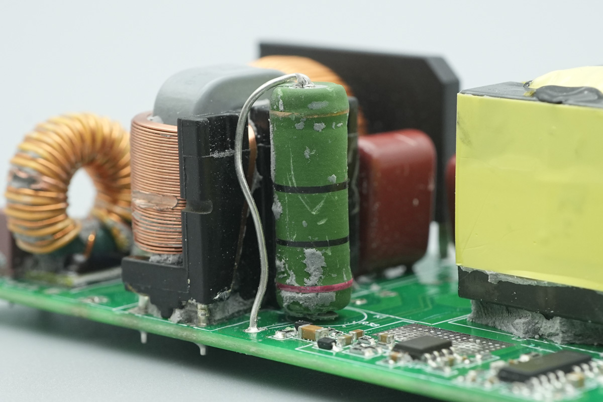
A color ring resistor.
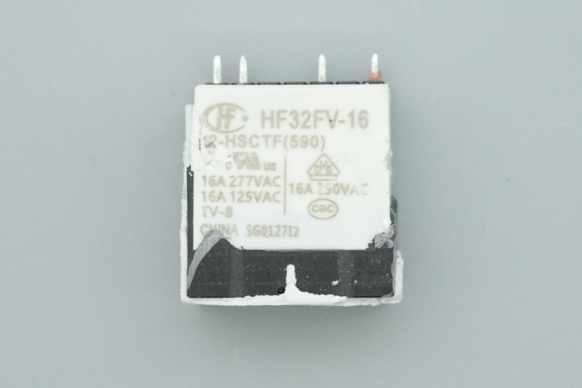
A relay from HONGFA, model HF32FV-16.
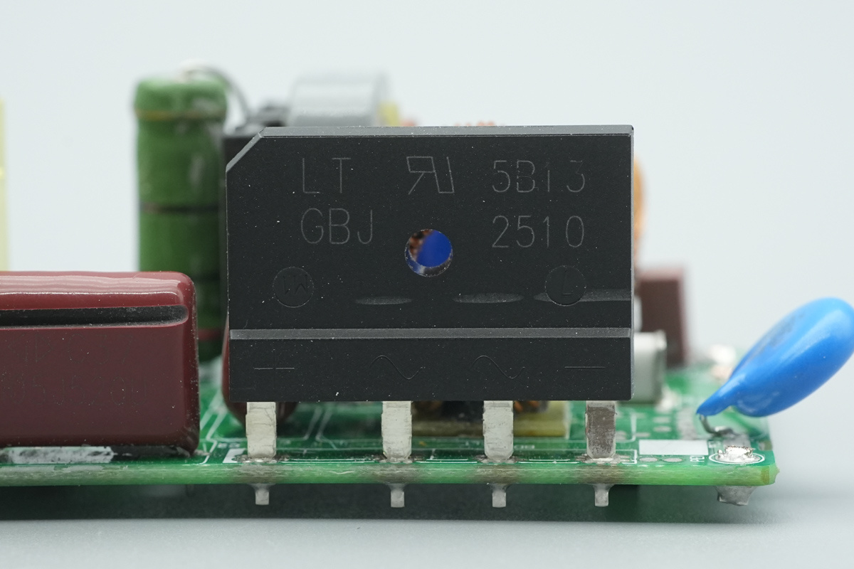
The rectifier bridge model is GBJ2510, rated at 25A 1000V, housed in a GBJ package.
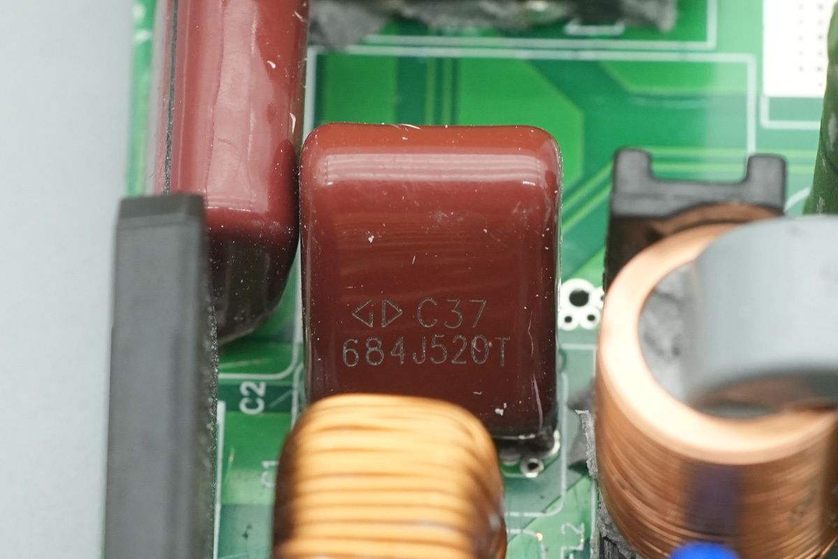
The film filtering cap is from Faratronic, spec 0.68μF 520V.
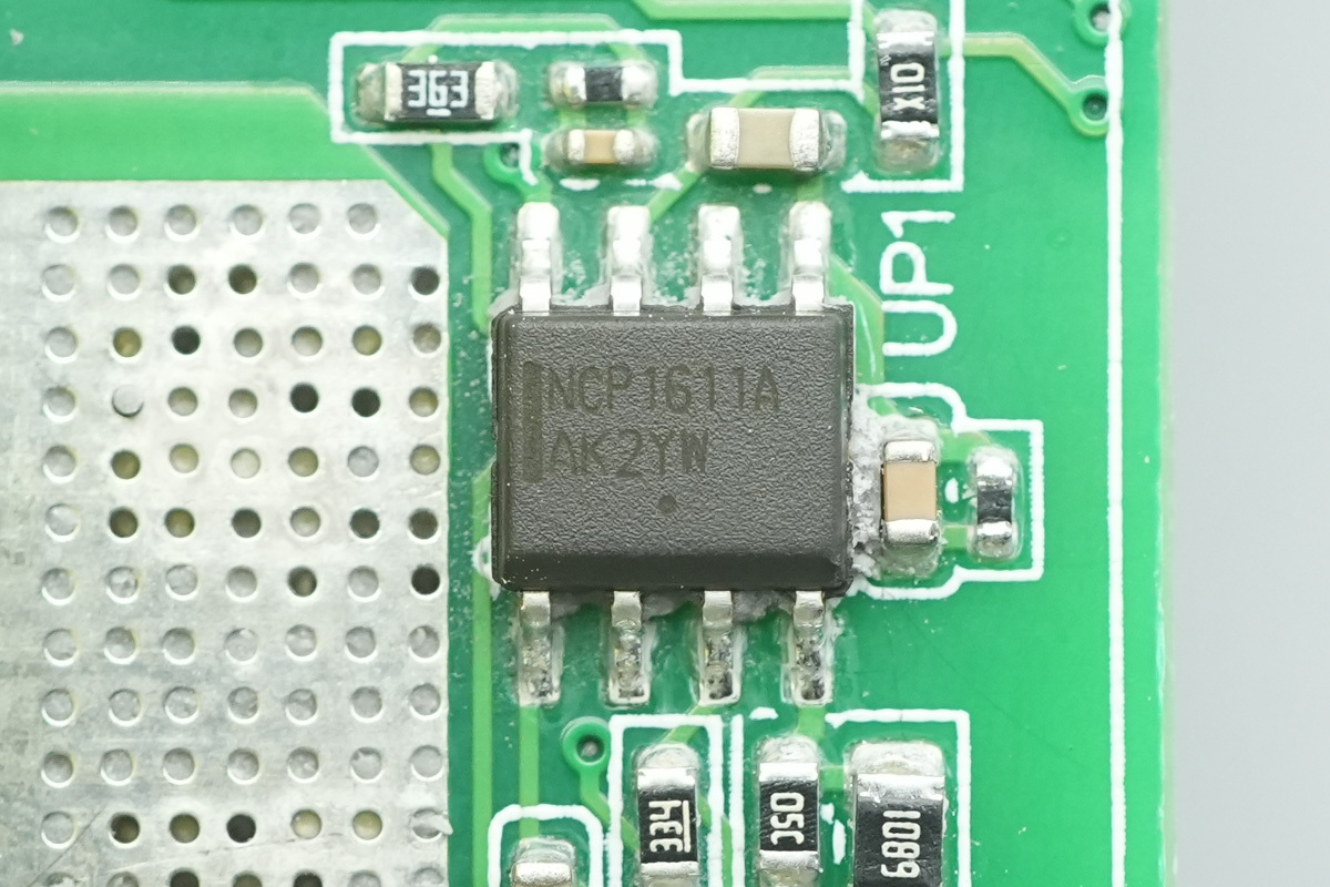
The PFC controller is from onsemi, model NCP1611A, housed in a SOP8 package, and specifically designed for AC-DC adapters, televisions, LED power supplies, and similar products.
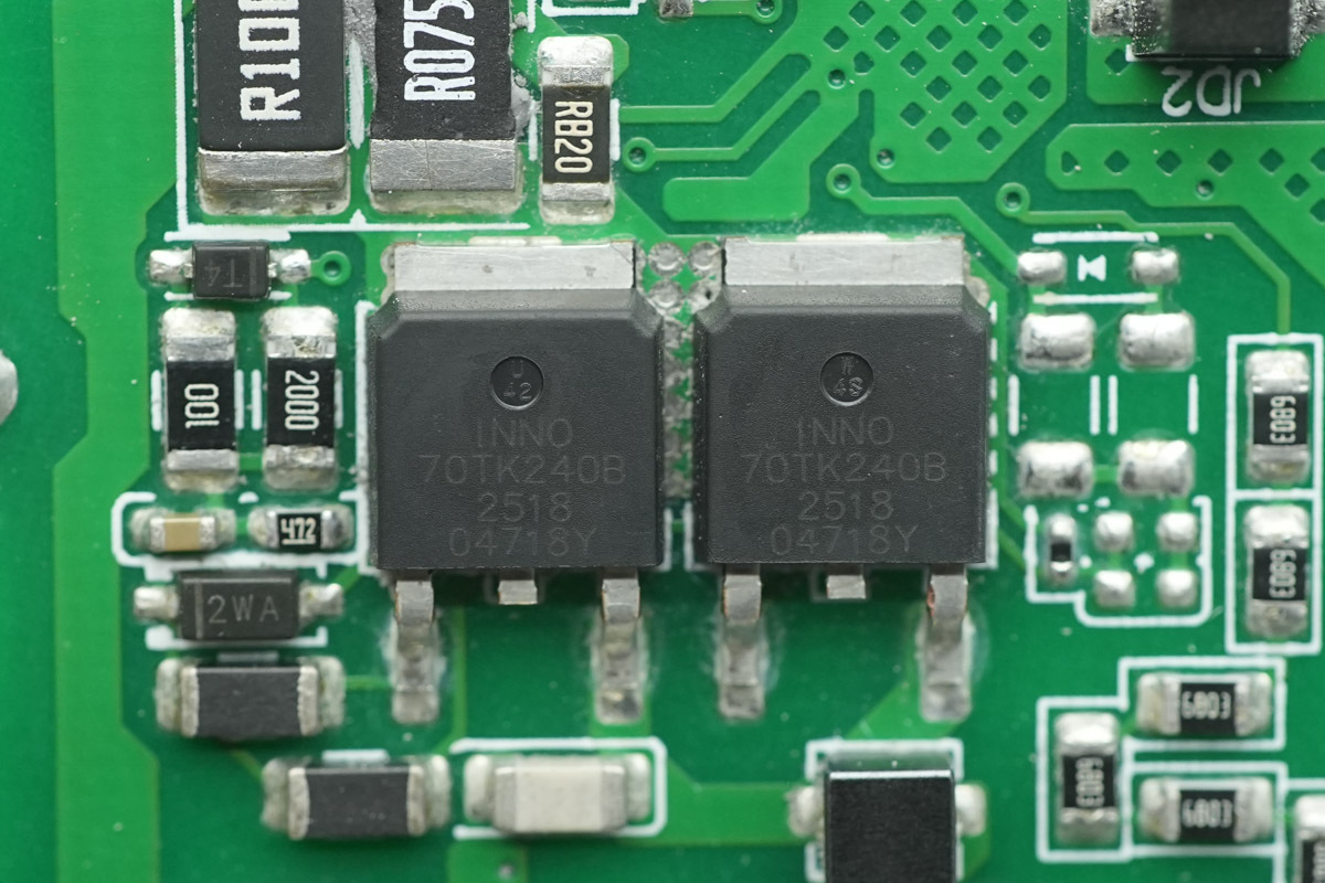
The PFC MOSFET is from Innoscience, model INN700TK240B. This is a 700V enhancement-mode GaN MOSFET with an 800V transient voltage rating and a 240mΩ on-resistance. It meets JEDEC standards for industrial applications, features built-in ESD protection, and adopts a TO252 package.
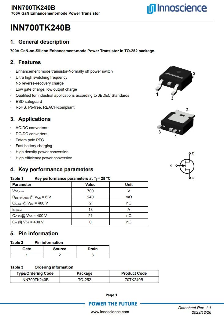
Here is the info about the Innoscience INN700TK240B.
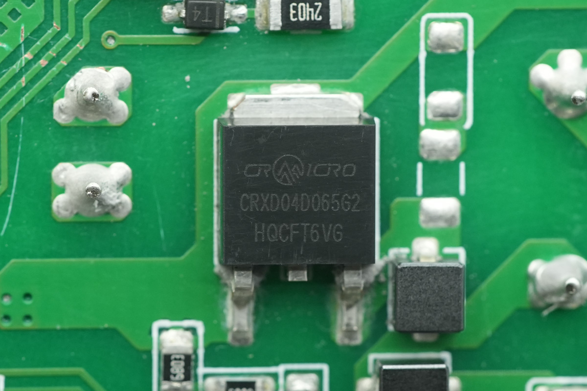
The PFC diode is from CRMICRO, which is a SiC diode, model CRXD04D065G2, rated at 650V 4A, housed in a TO-252 package.
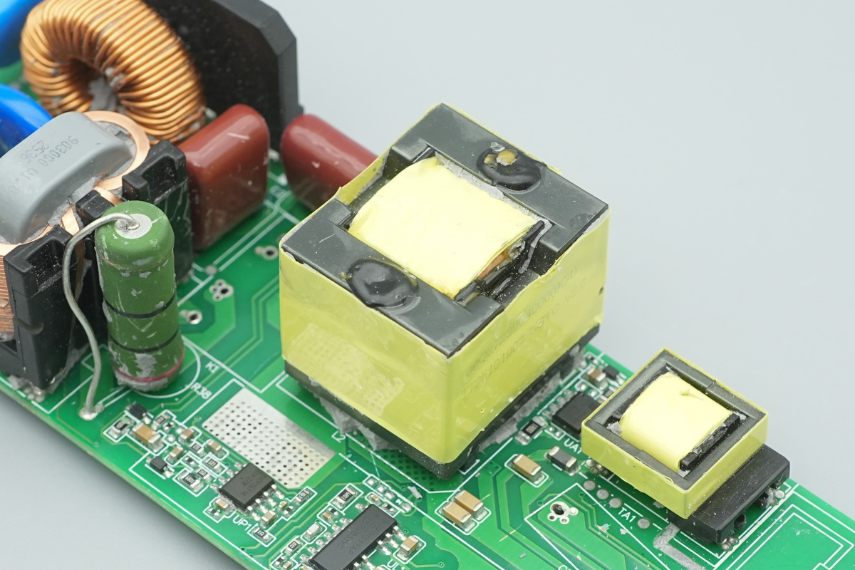
A PFC boost choke.
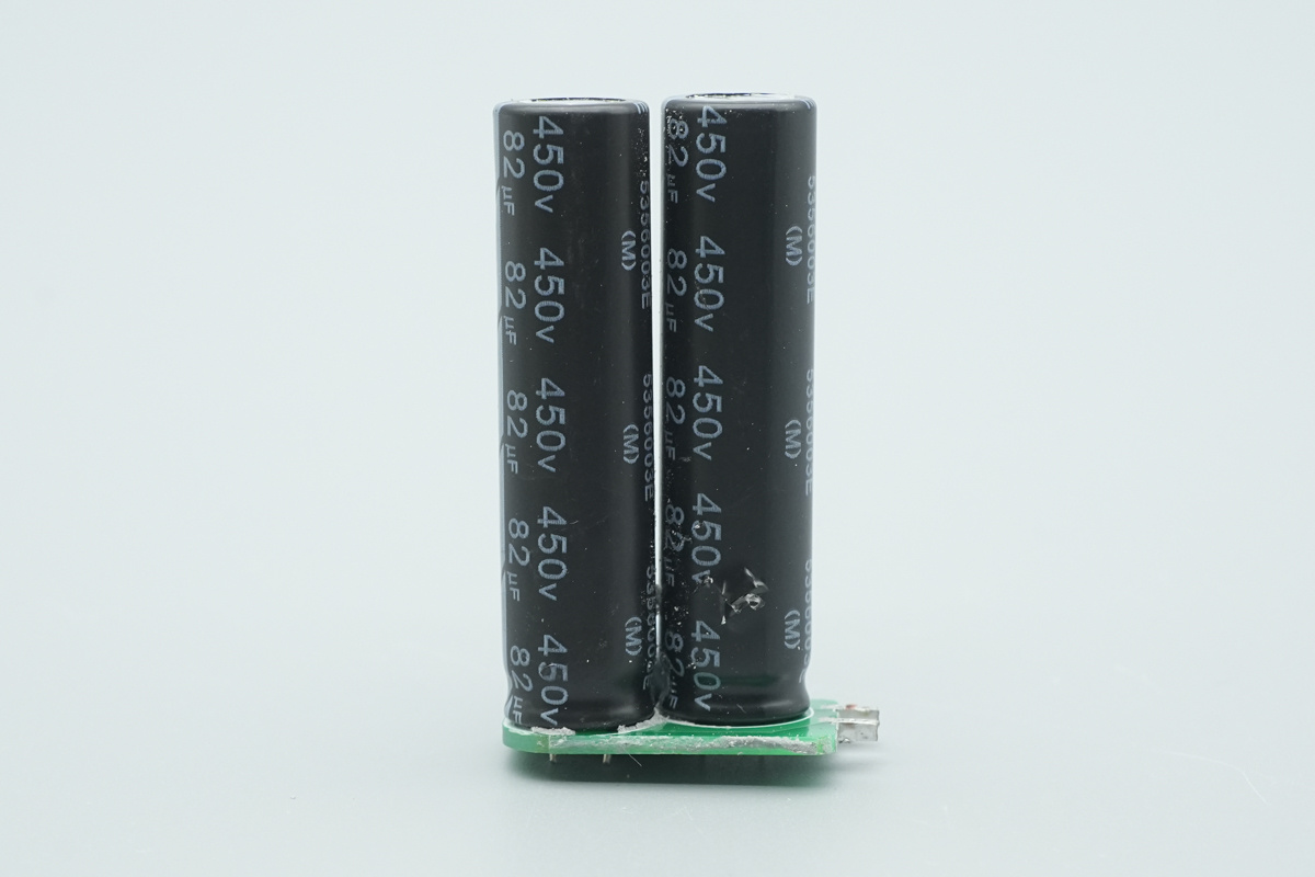
Two high-voltage filter caps are from JH, spec 450V 82μF.
Primary Master Control Circuit Analysis
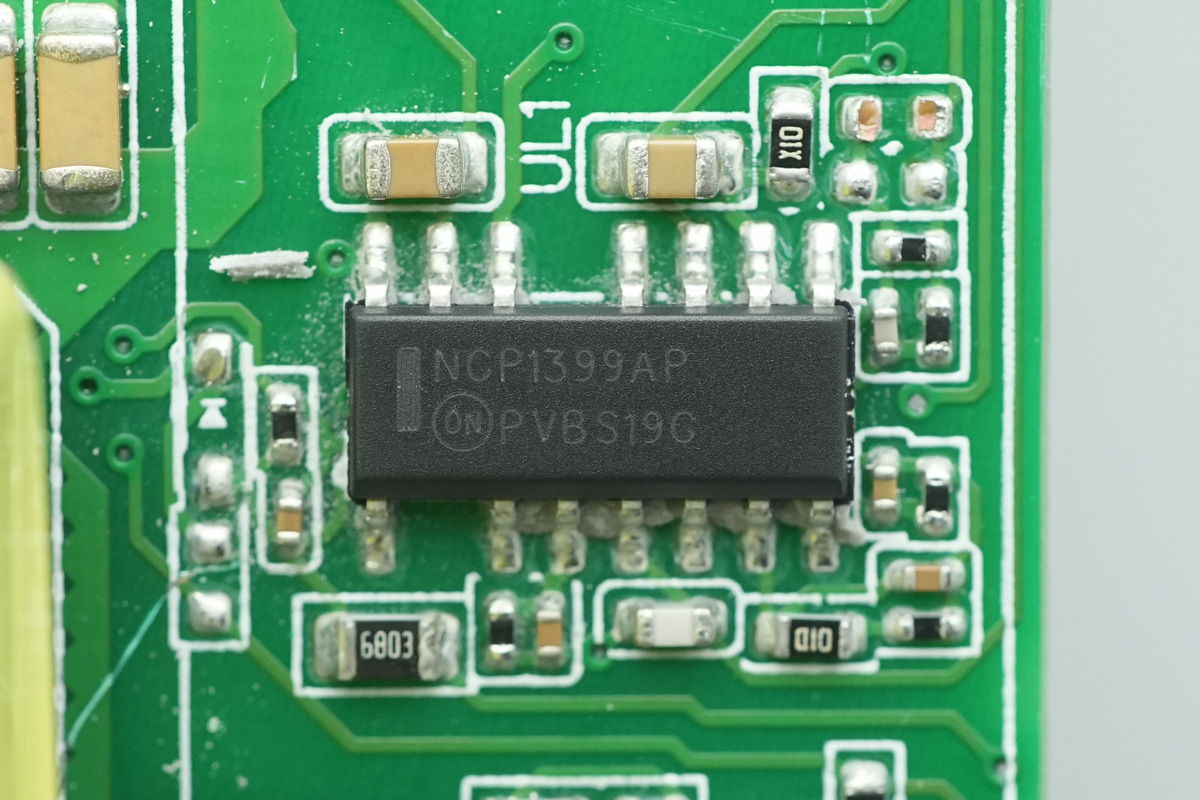
The primary master control chip is from onsemi, model NCP1399, housed in a SOIC-16 package. It is an LLC controller that integrates gate drivers, which simplifies layout and reduces the number of external components.
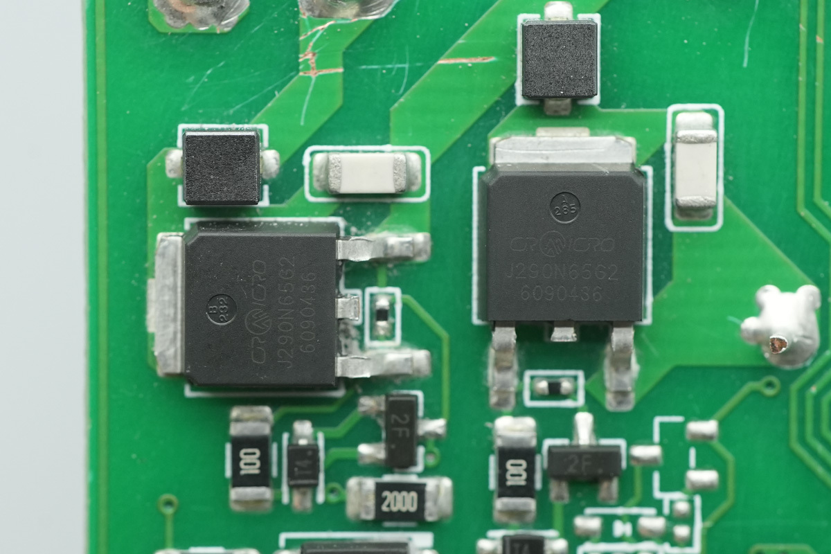
The primary switching MOSFET is from CRMICRO, marked J290N65G2, adopting a TO-252 package.
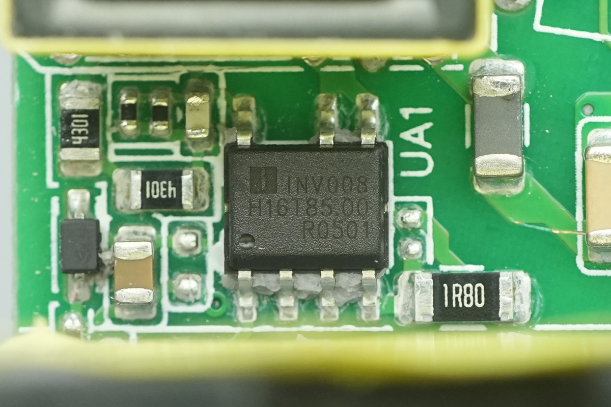
The auxiliary power supply chip, marked INV008.
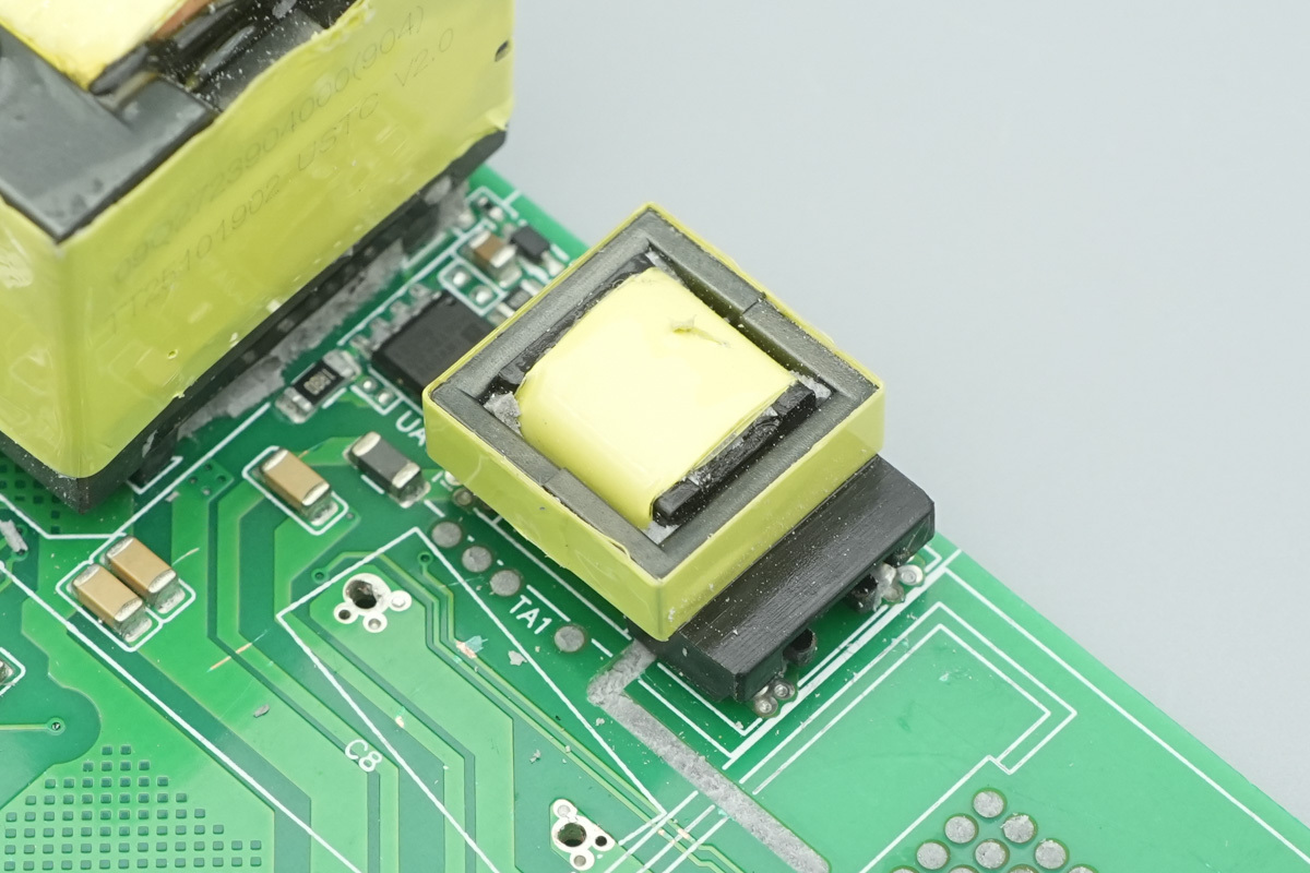
The auxiliary power supply transformer.
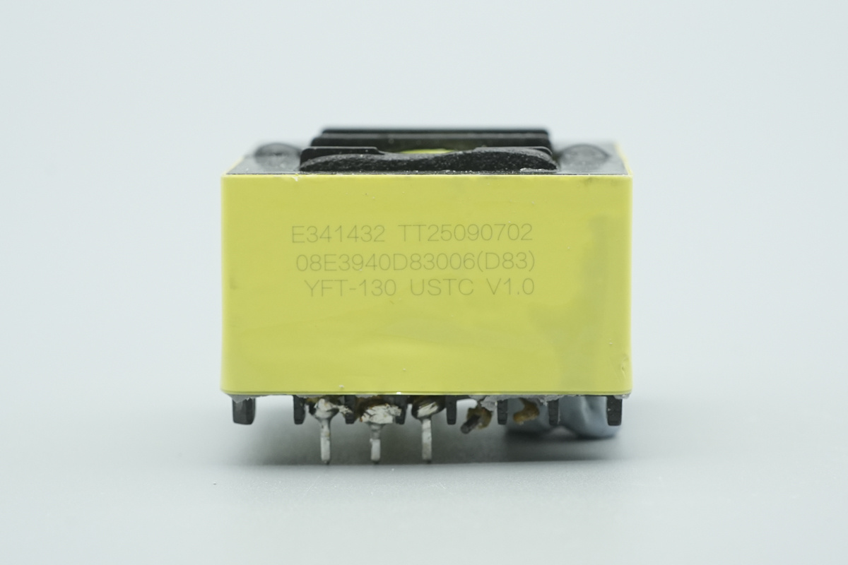
The transformer is marked with the code E341432 TT25090702.
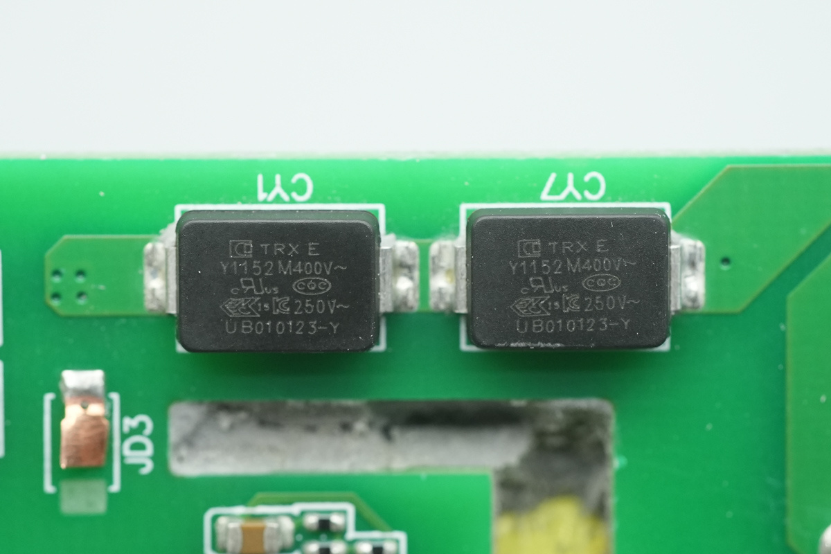
The two SMD Y-caps are from TRX, model TMY1152M,which feature a small size and lightweight design, making them ideal for high-density power products such as GaN fast chargers.
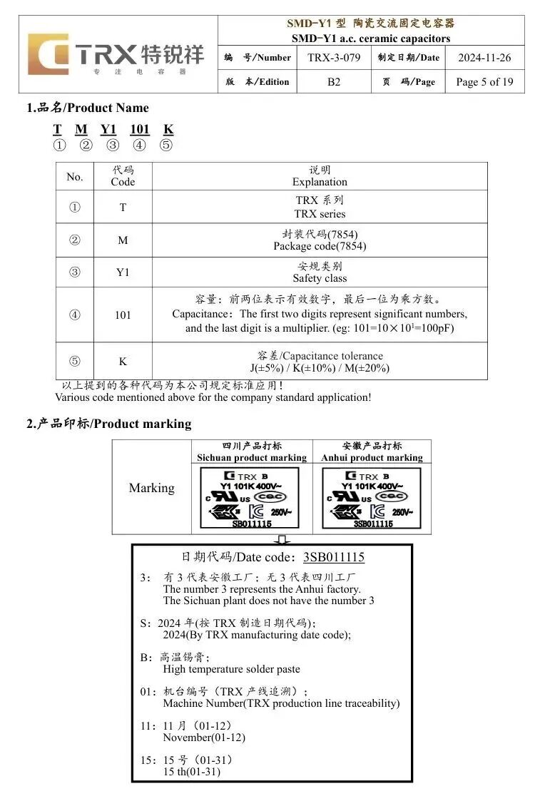
Here is the info about the TRX TMY1152M.
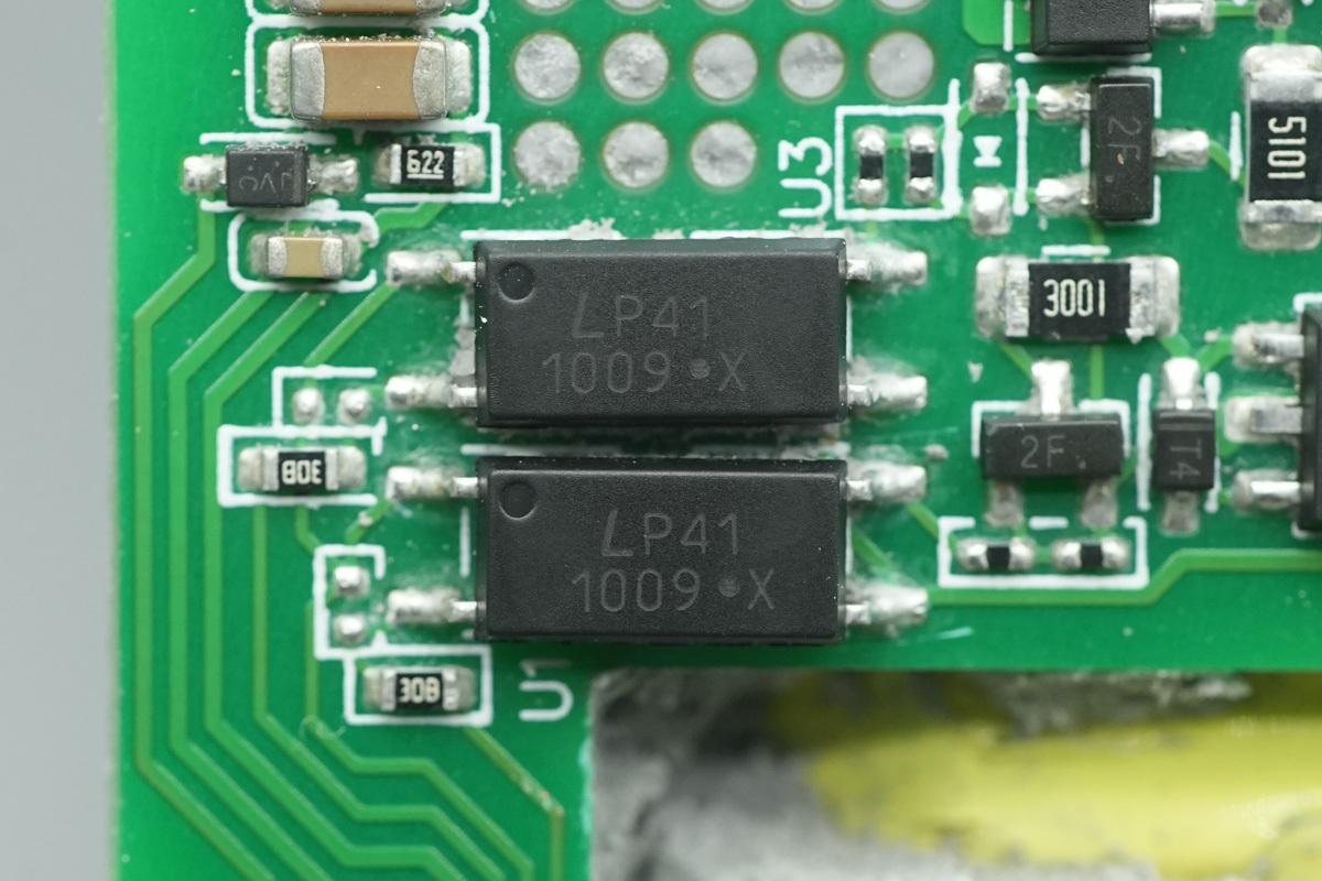
Two optocouplers, marked LP41.
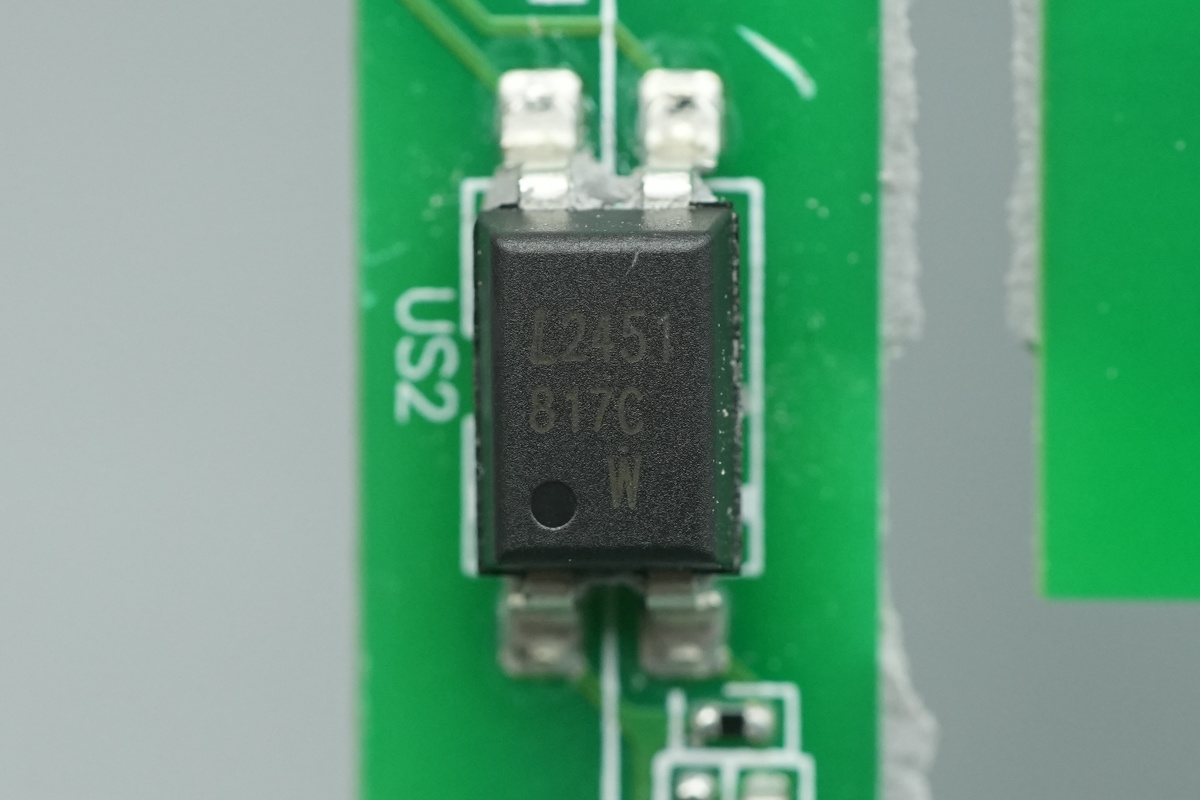
An optocoupler, marked L2451.
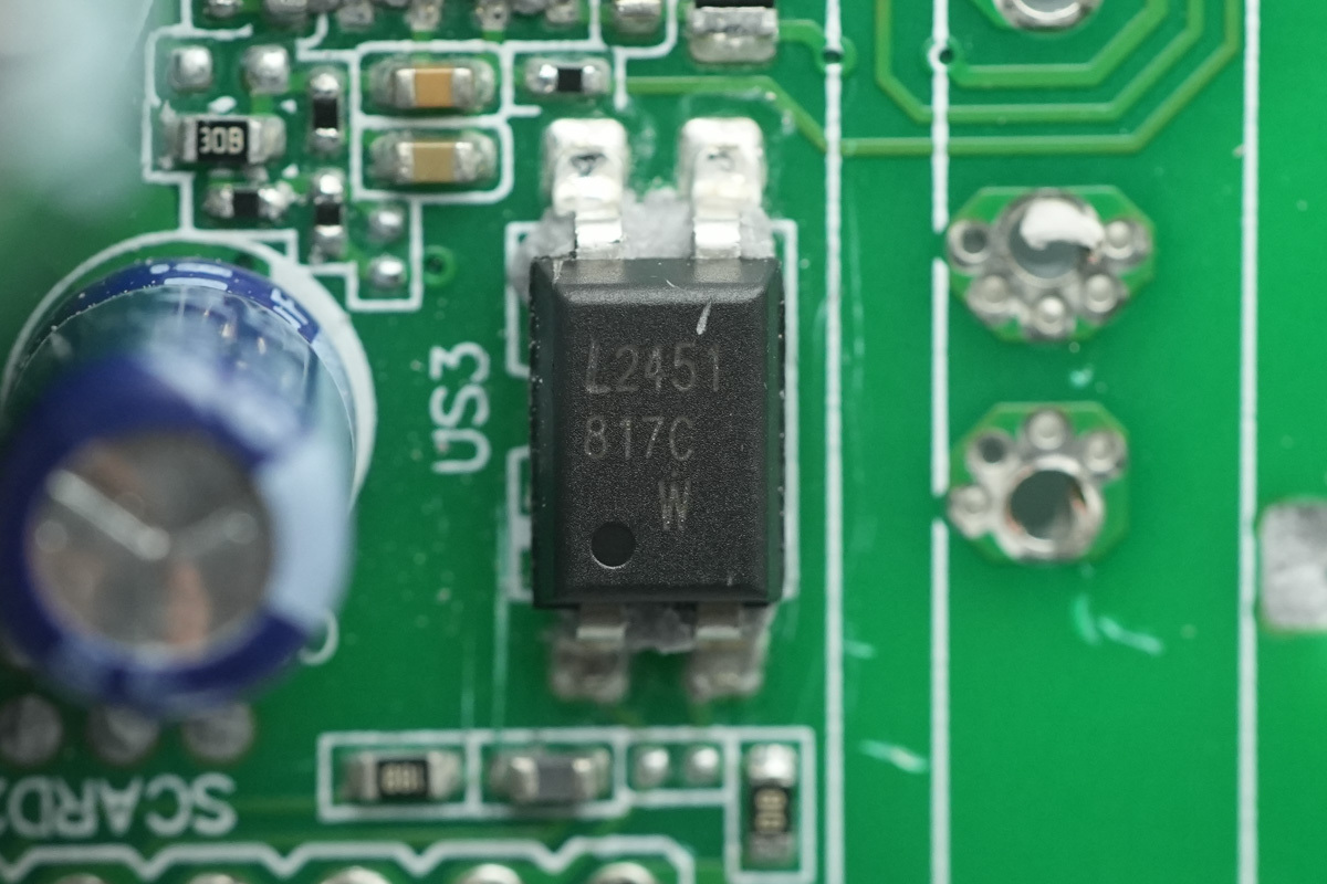
Another one with the same marking L2451.
Synchronous Rectification Circuit Analysis
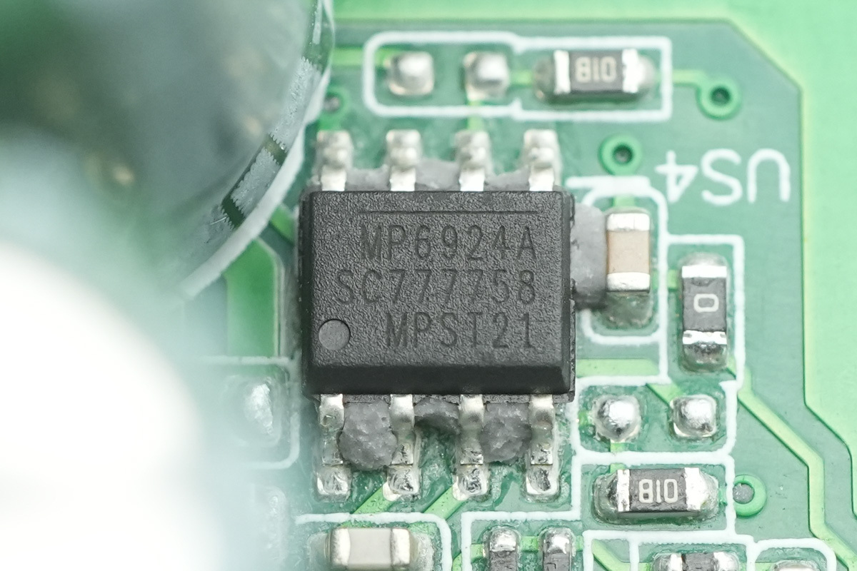
A synchronous rectifier chip from MPS, model MP6924A, housed in a SOIC8 package. It is a dual fast-turnoff intelligent rectifier designed for synchronous rectification in LLC topologies.
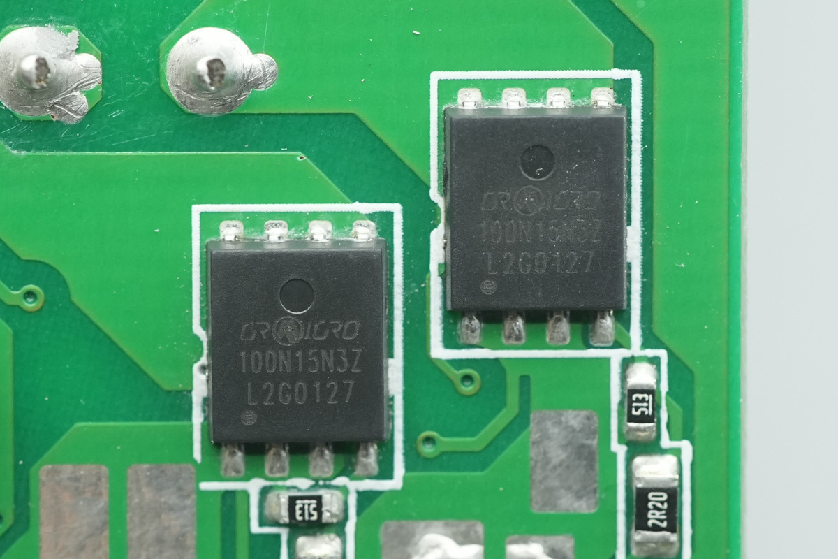
The secondary synchronous rectifier MOSFET is also from CRMICRO, model CRSM100N15N3Z, with a voltage rating of 150V, an on-resistance of 9.5mΩ, adopting a DFN5*6 package.
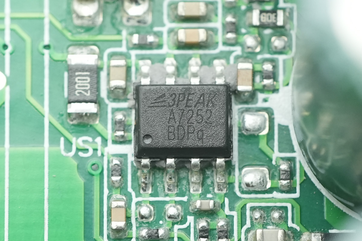
A dual operational amplifier from 3PEAK, model TPA7252, housed in a SOP8 package.
LED Power Supply Output Circuit Analysis
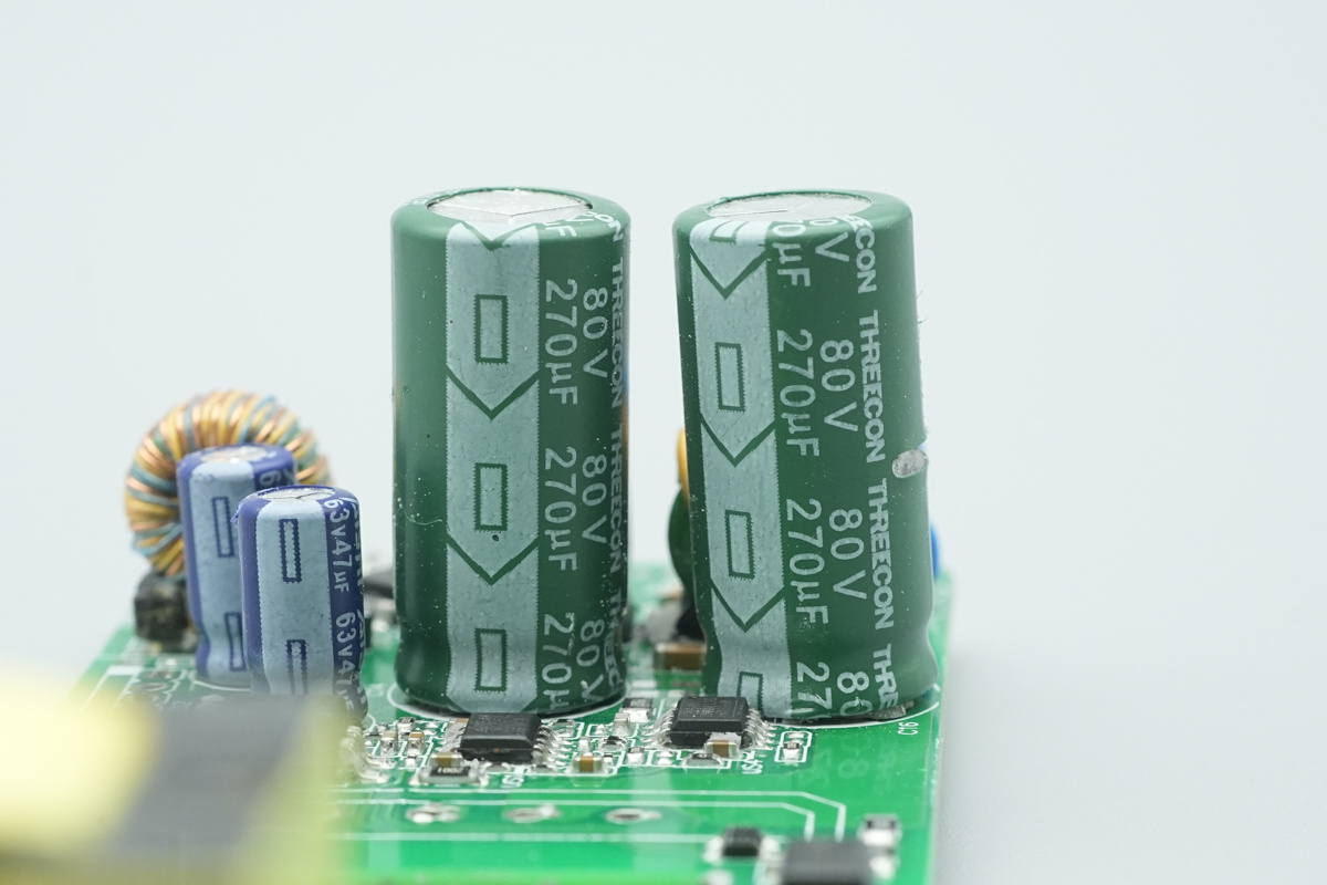
Two filtering electrolytic caps from THREECON, spec 80V 270μF.
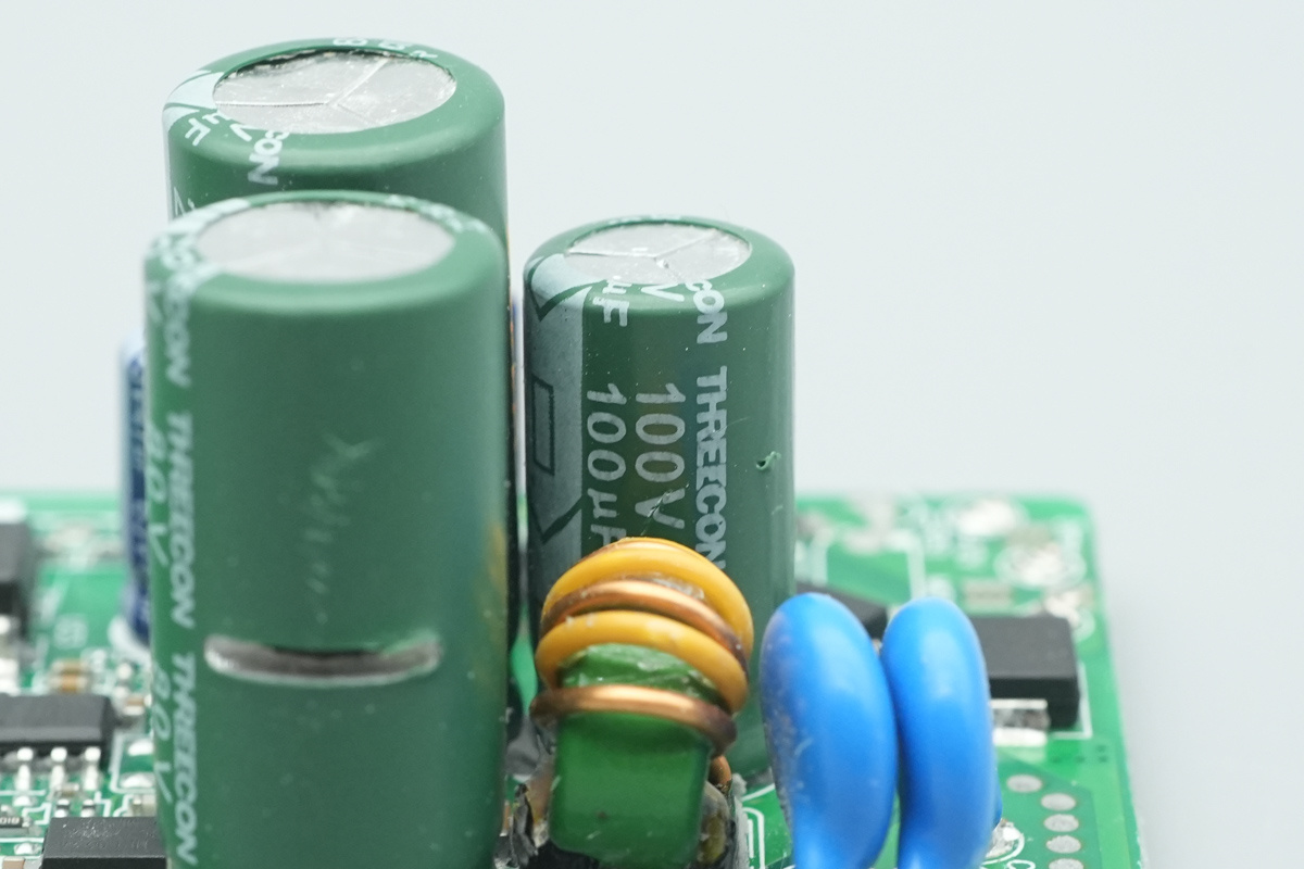
A filtering electrolytic cap from THREECON, spec 100V 100μF.
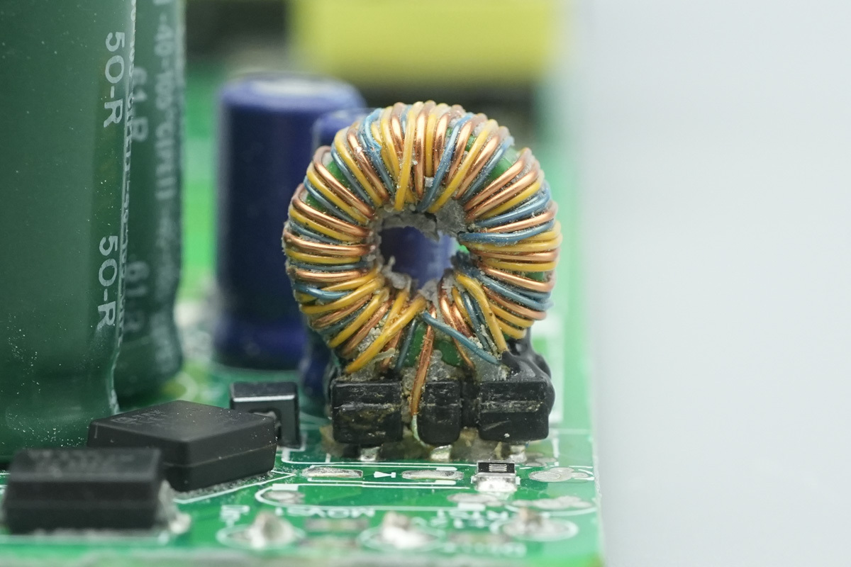
A toroidal filtering choke densely wound with multi-strand wires.
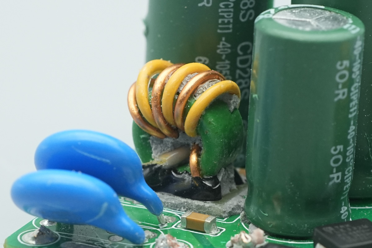
Another filtering choke.
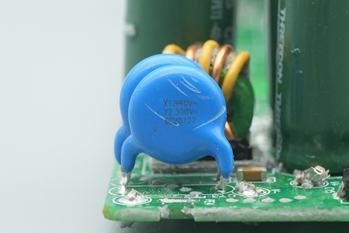
Two blue Y-caps located next to the output cable solder joints.
LED Dimming Control Circuit Analysis
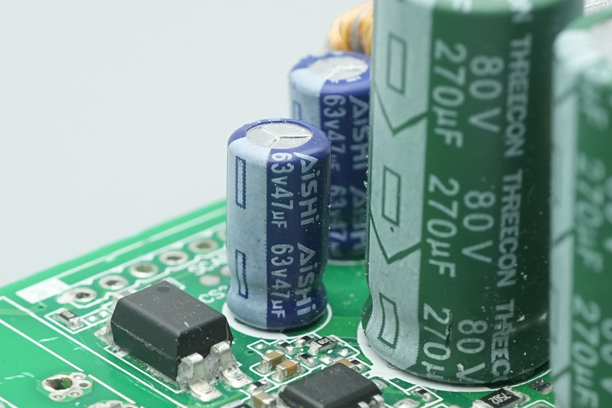
Two filtering caps are from AiSHi, spec 63V 47μF.
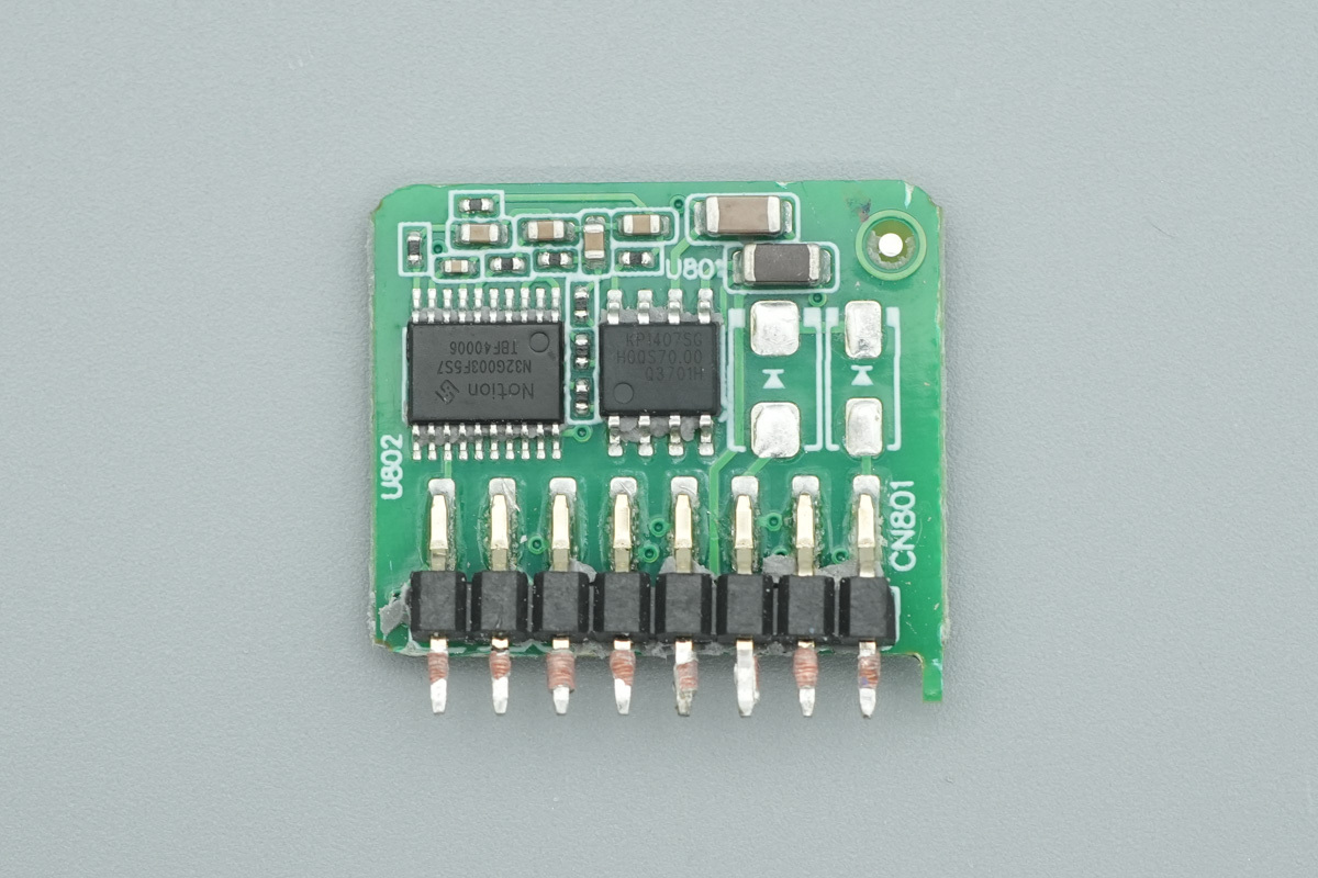
The dimming and control PCB.
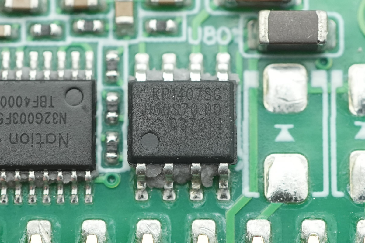
The dimming signal conversion auxiliary chip is from KIWI, model KP1407. It is a 0-10V/resistance/PWM dimming signal conversion auxiliary chip, mainly used in dimming LED driver power supplies, housed in a SOP-8 package.
It is highly compatible with the aforementioned dimming signals, enabling precise signal conversion and programmable control through cooperation with an MCU. Simultaneously, its pins also support UART serial communication at a baud rate of 57600bps, meeting the demand for low-latency data transmission.
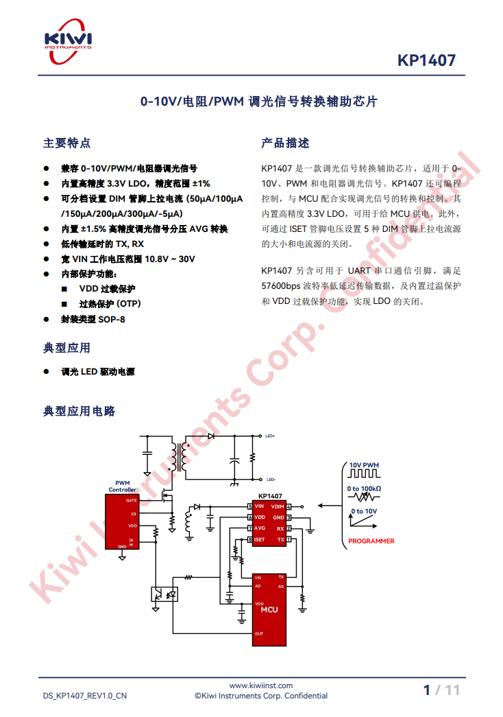
The chip features a wide operating voltage range of 10.8V to 30V and an integrated high-precision 3.3V LDO (±1% accuracy) capable of directly powering the MCU.
In addition, it integrates 5-level adjustable DIM pin pull-up currents and high-precision dimming signal voltage-divider conversion functions. It also incorporates VDD overload protection and OTP, effectively ensuring the stable and safe operation of the system.
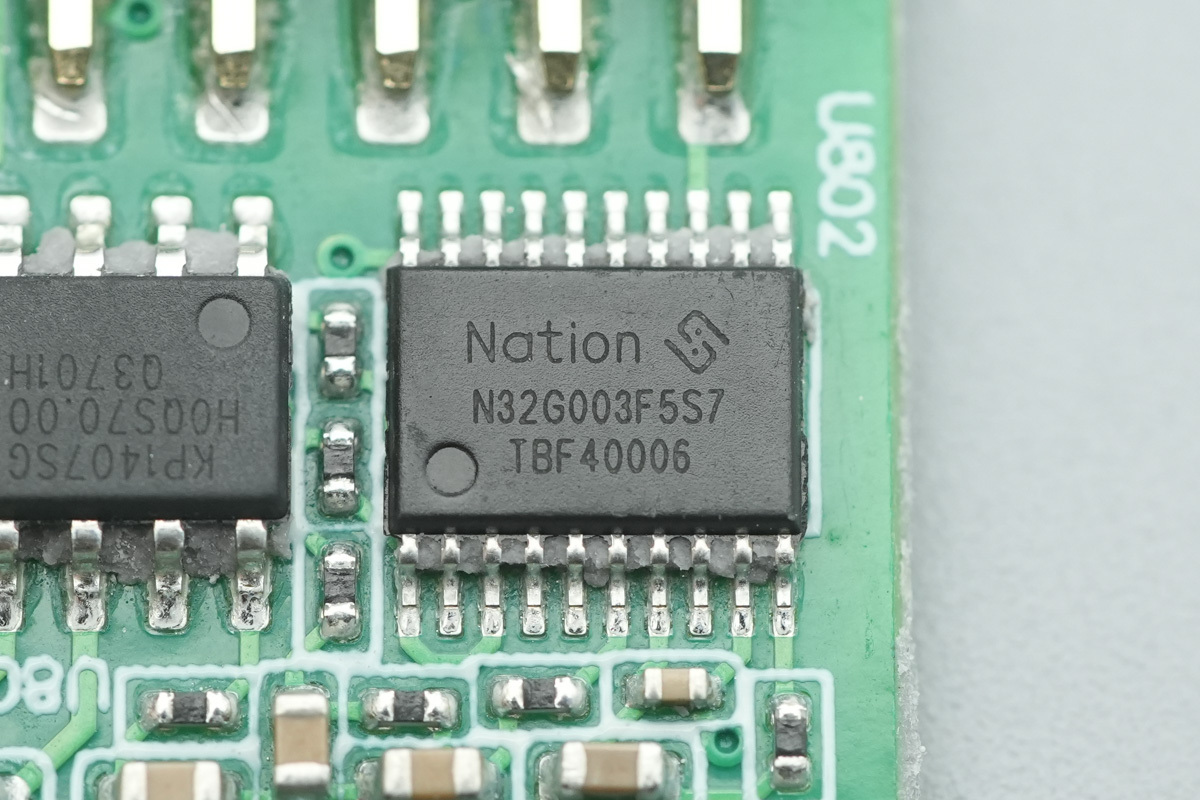
An MCU used for dimming control is from NSING, model N32G003F5S7, featuring an embedded 32-bit ARM Cortex-M0 core, 29.5 KB Flash, and 3 KB SRAM, housed in a TSSOP20 package. Working in conjunction with the KIWI KP1407, it can precisely process programmable dimming signals to achieve a more flexible intelligent dimming solution.
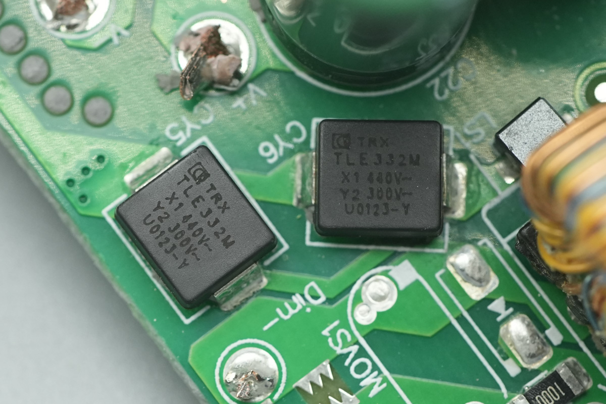
The SMD Y-cap is from TRX, model TGY2332ME. It features a small size and lightweight design, making it ideal for high-density power products such as GaN fast chargers.
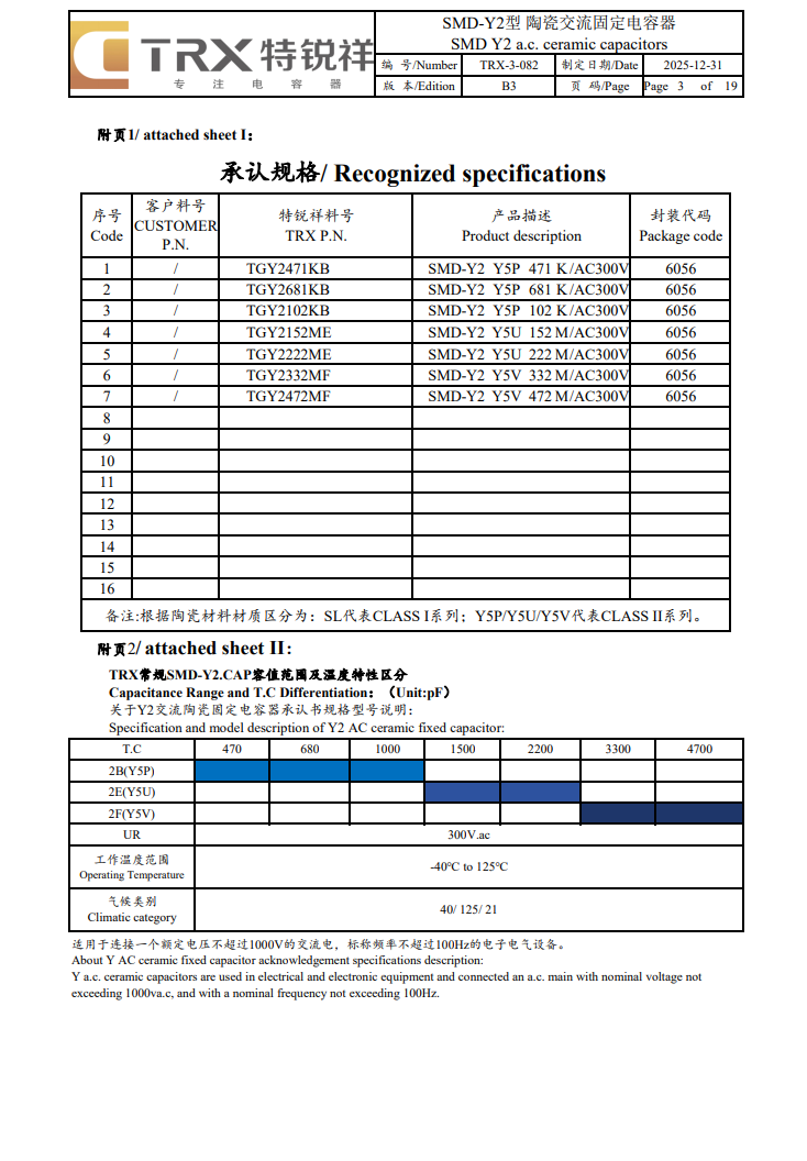
Here is the info about the TRX TGY2332ME.
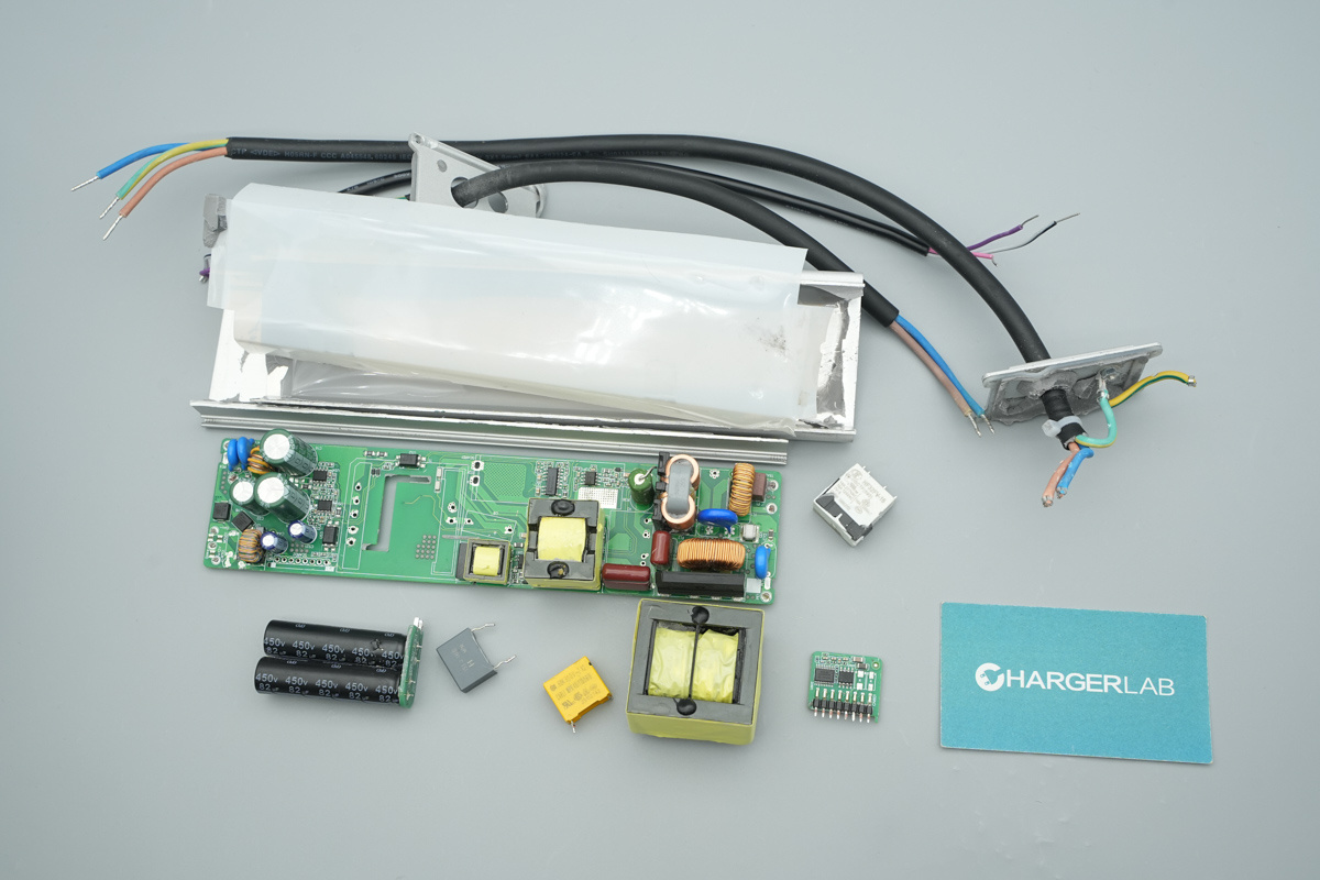
Well, those are all components of the Inventronics Programmable LED Control Power Supply.
Summary of ChargerLAB
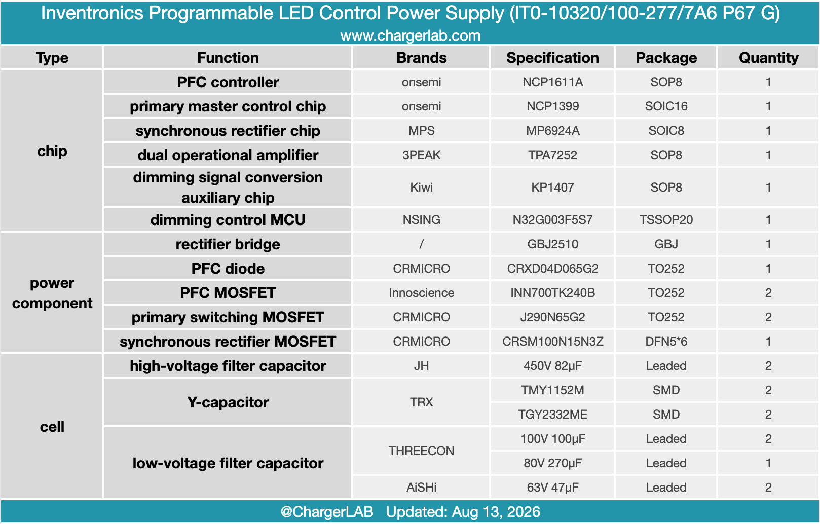
Through disassembly, ChargerLAB reveals that this programmable LED driver utilizes a robust extruded aluminum housing. The cable egress features heavy-duty dual sealing rubber gaskets, while the internal PCBA is fully potted with gray thermal compound. This high-grade protective engineering grants the unit formidable IP67-rated dust and water ingress protection.
Regarding circuitry and component selection, the power supply employs a high-efficiency PFC+LLC topology.
The primary stage integrates an onsemi NCP1611A PFC controller with an Innoscience 700V enhancement-mode GaN power MOSFET and a CRMICRO SiC diode. Primary control is handled by an onsemi NCP1399 paired with a CRMICRO primary MOSFET. The secondary rectification stage relies on an MPS MP6924A controller and a CRMICRO MOSFET (marked J290N65G2).
Furthermore, to support flexible programmable dimming, an independent PCB houses an NSING 32-bit MCU and a KIWI KP1407 dimming signal converter.
In summary, this Inventronics LED power supply is engineered for extreme environments, ensuring long-term, reliable operation in harsh outdoor conditions characterized by heavy dust and high humidity.